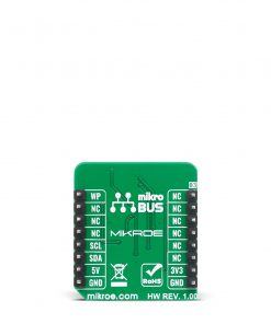
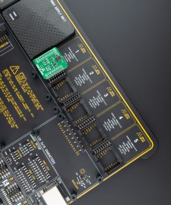
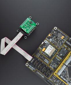
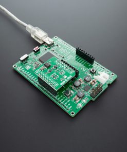
SRAM 2 Click
R335.00 ex. VAT
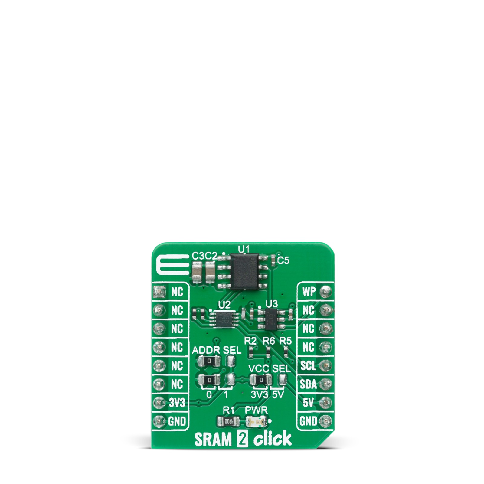
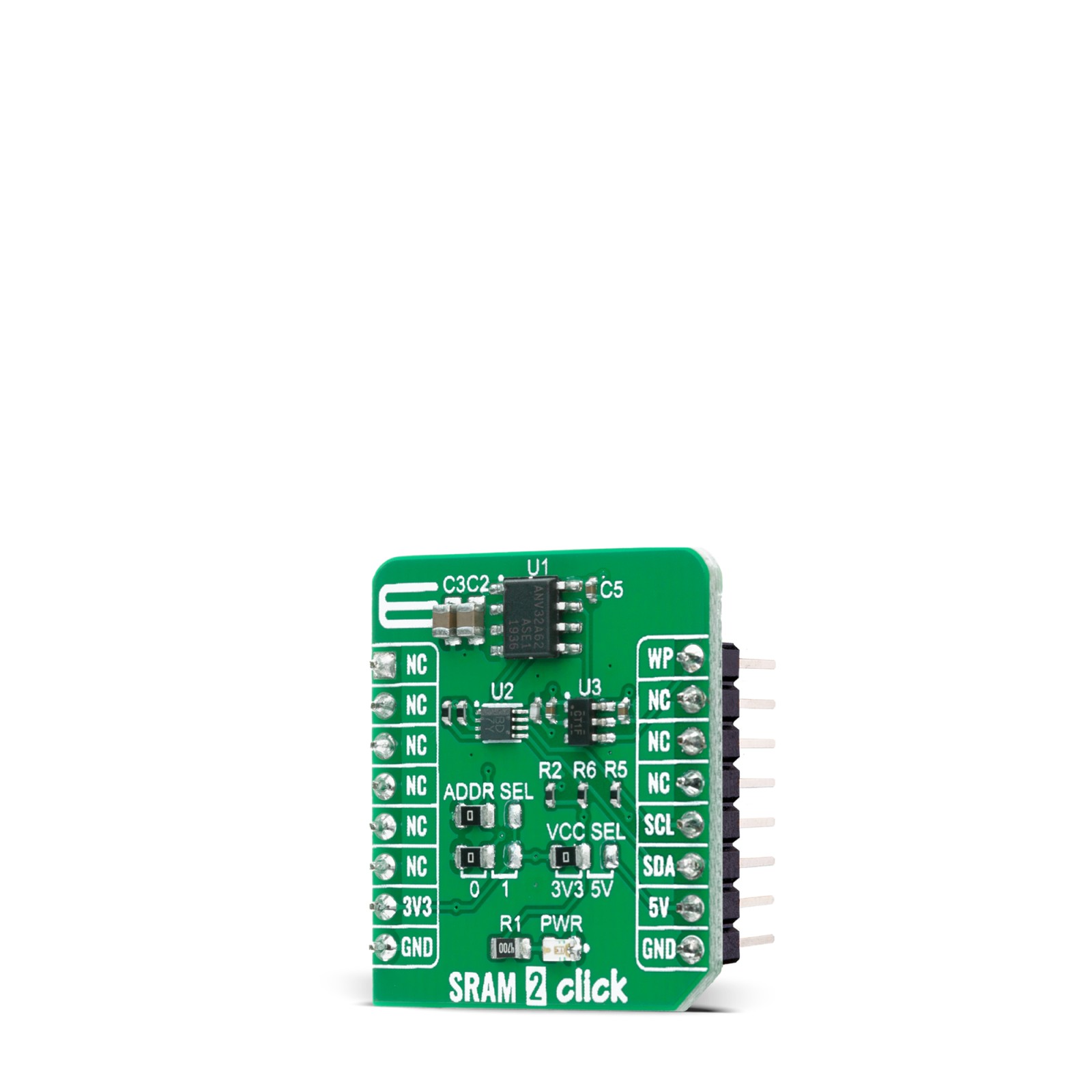
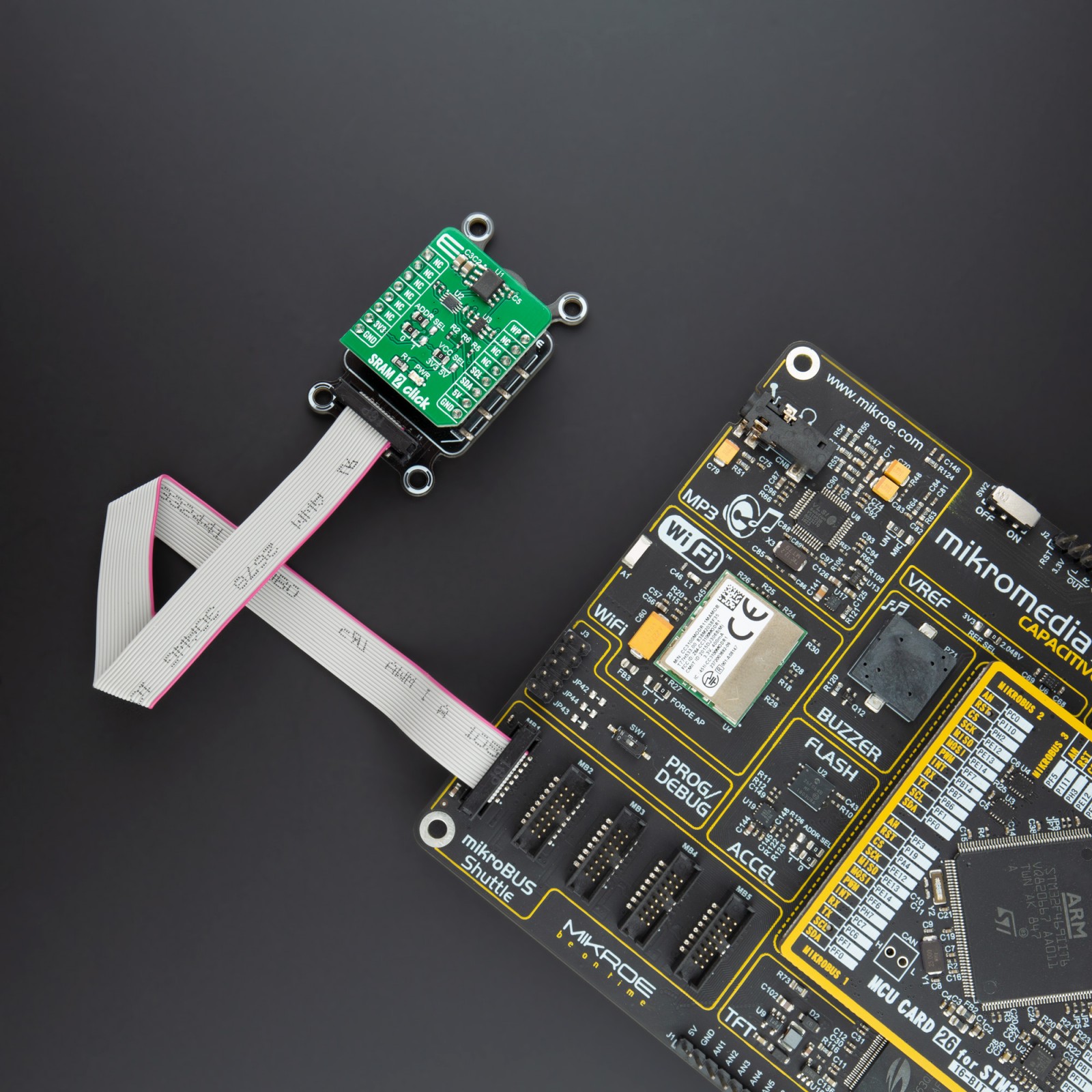
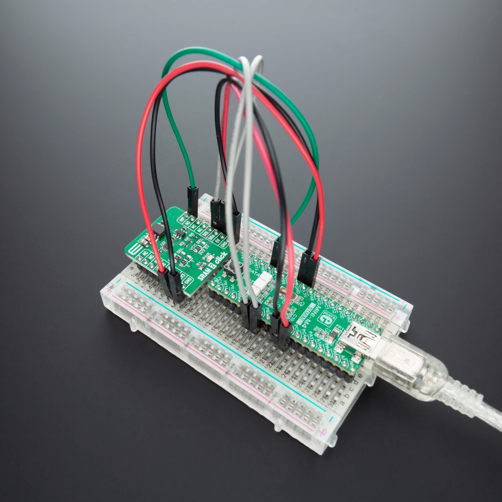
SRAM 2 Click is based on ANV32A62A SRAM memory from Anvo-Systems Dresden. It’s a 64Kb serial SRAM with a non-volatile SONOS storage element included with each memory cell, organized as 8k words of 8 bits each. Communication is done by a I²C with up to 4 cascadable devices that can share the common bus. The serial nvSRAM provides the access and cycle times, easy to use and unlimited read and write endurance of a SRAM. This Click board™ can be easily used to store drive profiles, configurations and similar data, which are typically stored in a FLASH.
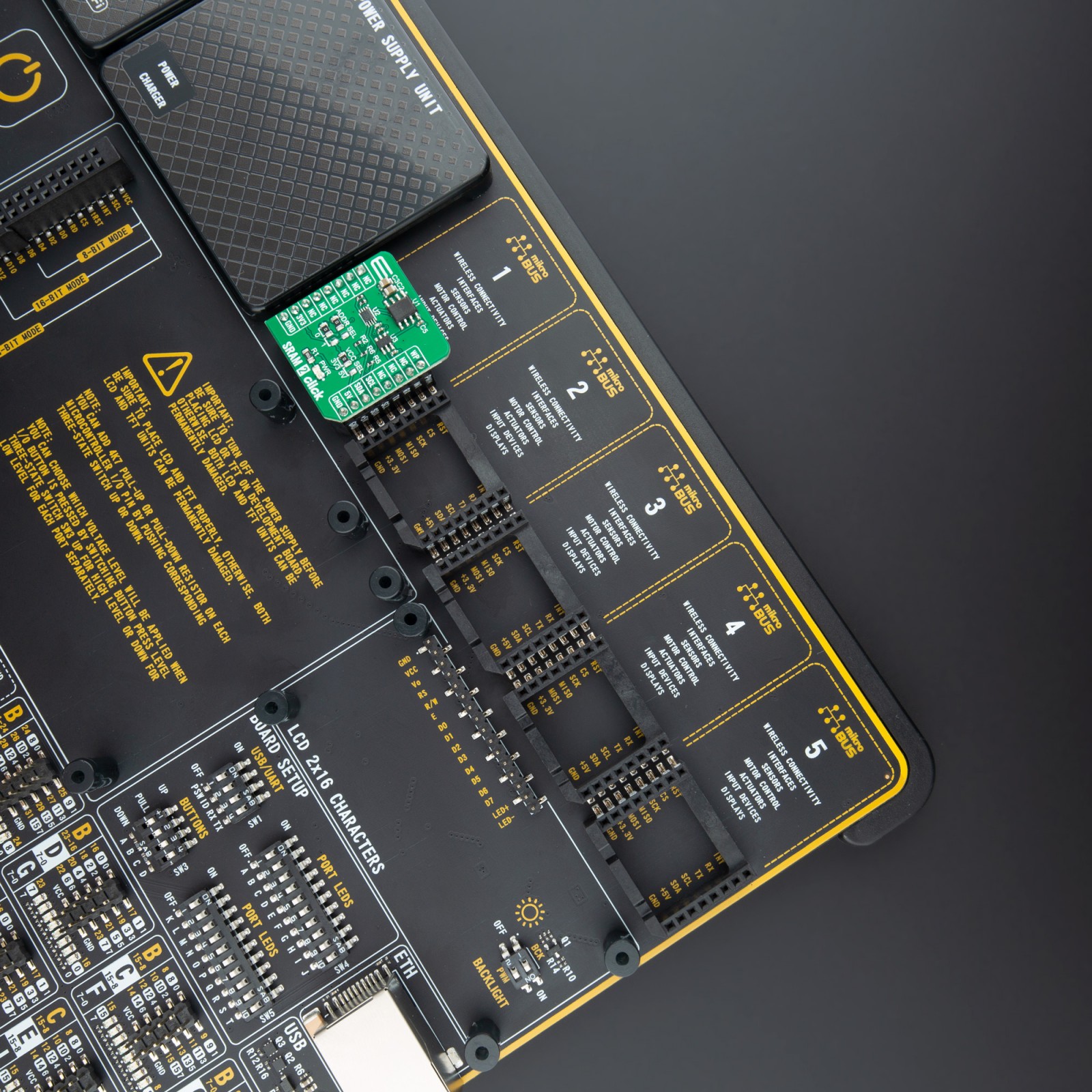
SRAM 2 Click board™ is supported by a mikroSDK compliant library, which includes functions that simplify software development. This Click board™ comes as a fully tested product, ready to be used on a system equipped with the mikroBUS™ socket.
Stock: Lead-time applicable.
| 5+ | R318.25 |
| 10+ | R301.50 |
| 15+ | R284.75 |
| 20+ | R274.03 |
How does it work?
SRAM 2 Click is using nvSRAM which is ordinary SRAMs with the ability for self-sufficient, automatic backup of SRAM-data in an internal FLASH, All Read/Write operations are addressing the SRAM array only. From a user point of view, nvSRAM appears as ordinary SRAM. SRAM are fast, energy efficient and does not wear-out while R/W operations. This explains the superior speed and the unlimited R/W endurance of nvSRAM. Data transfers automatically to the non-volatile storage cells when power loss is detected or in any brown out situation (PowerStore). As long as power will be supplied within operating conditions all data stay volatile in the SRAM cells.
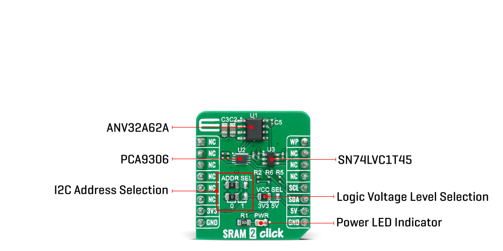
SRAM 2 Click is using a standard two-wire interface (I²C) and is functional similar to serial EEPROMs or FRAM . The addressing requires a 13 bit address out of the 2-byte address of the two-wire protocol. The jumpers ADDR SEL are device address inputs to select 1 of up to 4 devices of the same type on the same I²C bus. To select one device the hard wired addresses on the 2 pins have to match with the related bits in the slave address.
This SRAM also features PowerStore operation which is a unique feature of the SONOS technology that is enabled by default on the ANV32A62A. During normal operation, the device will draw current from VCC for circuit operation and to charge a capacitor connected to the VCAP pin. This stored charge will be used by the chip to perform a single STORE operation in case of power down. If the voltage on the VCC pin drops below VSWITCH, the part will automatically disconnect the VCAP pin from VCC. A STORE operation will be initiated with power provided by the VCAP capacitor.
If a write operation is in progress all data of complete written pages are valid. Only the last incomplete written byte will be ignored. With the following Power Store execution these data become non-volatile. To reduce needless non-volatile stores, Power Store operation will be ignored unless at least one write operation has taken place since the most recent STORE cycle. The PowerStore Operation is valid for the complete memory array.
SRAM 2 click is powered via the mikroBUS™ 3.3V rail. However, it offers a logic voltage selection, via the VCC SEL jumper. Since the ANV32A62A memmory cannot operate with signals up to 5V, a level shifting IC is used to allow both 3.3V and 5V MCUs to be interfaced with this Click board™. The VCC SEL jumper routes either 3.3V or 5V to the voltage reference pin of the PCA9306, a dual bidirectional level shifting IC.
Specifications
Type
SRAM
Applications
Workstations, Routers, Peripheral equipment, and other lpw-power applicatins
On-board modules
HSFPAR003A
Key Features
Unlimited READ and WRITE Cycles, 100-Year Non-volatile Data Retention, Hardware Write-Protect
Interface
I2C
Feature
No ClickID
Compatibility
mikroBUS™
Click board size
S (28.6 x 25.4 mm)
Input Voltage
3.3V or 5V
Pinout diagram
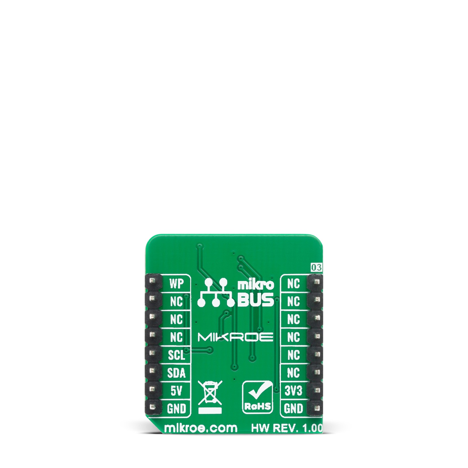
This table shows how the pinout on SRAM 2 Click corresponds to the pinout on the mikroBUS™ socket (the latter shown in the two middle columns).
Onboard settings and indicators
| Label | Name | Default | Description |
|---|---|---|---|
| PWR | LD1 | – | Power LED Indicator |
| VCC SEL | JP1 | Left | Logic level voltage selection: left position 3V3, right position 5V |
| ADDR1 | JP2 | Left | Slave address selection: Left position 0, right position 1. |
| ADDR2 | JP3 | Left | Slave address selection: Left position 0, right position 1. |
Software Support
We provide a library for the SRAM 2 Click on our LibStock page, as well as a demo application (example), developed using MikroElektronika compilers. The demo can run on all the main MikroElektronika development boards.
Library Description
Library provides control over reading and writing data via I2C module. You can use 2 specific functions for reading and writing to memory.
Key functions:
void sram2_write_protect( uint8_t state )– Write protect data selectionvoid sram2_write_memory( uint16_t addr, uint8_t wr_data )– Generic write data functionuint8_t sram2_read_memory( uint16_t addr )– Generic read data function
Examples description
The application is composed of three sections :
- System Initialization – Initializes I2C module
- Application Initialization – Initializes driver init
- Application Task – Writes and then reads data from memory
void application_task ( )
{
     uint8_t cnt;

     mikrobus_logWrite( ">> Write data [MikroE] to memory.", _LOG_LINE );
     sram2_write_protect( SRAM2_WR_ENABLE );
     for ( cnt = 0; cnt < 8; cnt++ )
     {
         sram2_write_memory( memory_addr + cnt, message_data[ cnt ] );
     }
     Delay_ms( 1000 );
     sram2_write_protect( SRAM2_WR_DISABLE );
     mikrobus_logWrite( ">> Read data from memory. Data : ", _LOG_TEXT );
     for ( cnt = 0; cnt < 8; cnt++ )
     {
         rx_data = sram2_read_memory( memory_addr + cnt );
         mikrobus_logWrite( &rx_data, _LOG_BYTE );
         mikrobus_logWrite( " ", _LOG_TEXT );
         Delay_100ms();
     }
     mikrobus_logWrite( " ", _LOG_LINE );
     mikrobus_logWrite( "--------------------------------", _LOG_LINE );
     Delay_ms( 2000 );
}
The full application code, and ready to use projects can be found on our LibStock page.
Other mikroE Libraries used in the example:
- I2C Library
- UART Library
Additional notes and informations
Depending on the development board you are using, you may need USB UART click, USB UART 2 click or RS232 click to connect to your PC, for development systems with no UART to USB interface available on the board. The terminal available in all MikroElektronika compilers, or any other terminal application of your choice, can be used to read the message.
mikroSDK
This Click board™ is supported with mikroSDK – MikroElektronika Software Development Kit. To ensure proper operation of mikroSDK compliant Click board™ demo applications, mikroSDK should be downloaded from the LibStock and installed for the compiler you are using.
For more information about mikroSDK, visit the official page.
Resources
Downloads
| Weight | 16 g |
|---|---|
| Brand | MikroElektronika |

