SQI FLASH Click
R310.00 ex. VAT
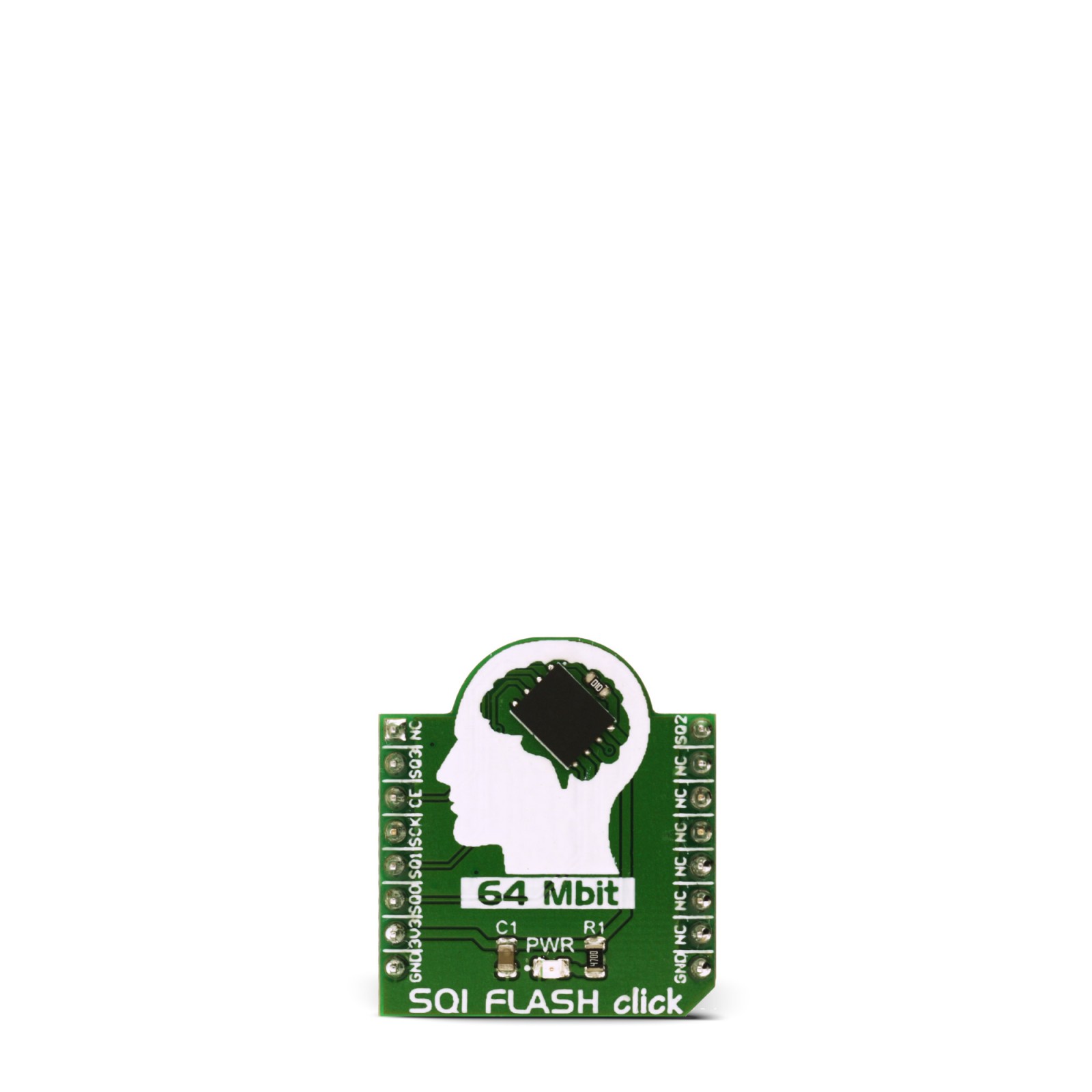
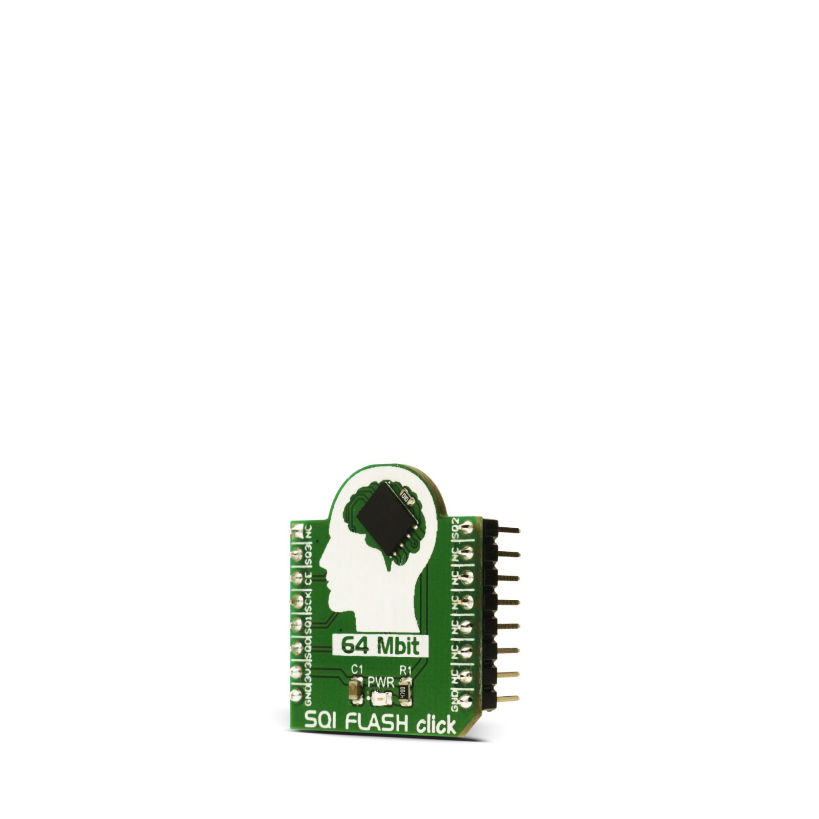
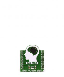
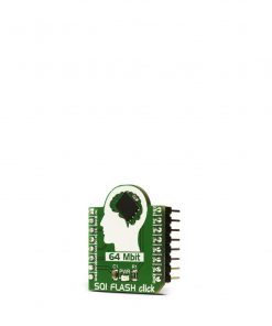
SQI FLASH click is based on the SST26VF064B, a 64 Mbit Serial Quad I/O flash device from Microchip. The chip utilizes 4-bit multiplexed I/O serial interface to boost the performance. The click is a very fast solid-state, non-volatile data storage medium, that can be electrically erased and reprogrammed. Operating at 104 MHz, the SST26VF064B enables minimum latency execute-in-place (XIP) capability, without the need for the code shadowing.
Features like the high performance and reliability, make the SQI Flash click the ideal choice for network appliances, DSL and cable modems, wireless network devices, automotive and any other applications, where high-speed reliable data storage is needed. Further benefits are achieved with its proprietary, high-performance CMOS SuperFlash® technology, which significantly improves the performance and reliability and lowers the power consumption.
Stock: Lead-time applicable.
| 5+ | R294.50 |
| 10+ | R279.00 |
| 15+ | R263.50 |
| 20+ | R253.58 |
SQI FLASH click is based on the SST26VF064B, a 64 Mbit Serial Quad I/O flash device from Microchip. The chip utilizes 4-bit multiplexed I/O serial interface to boost the performance. The click is a very fast solid-state, non-volatile data storage medium, that can be electrically erased and reprogrammed. Operating at 104 MHz, the SST26VF064B enables minimum latency execute-in-place (XIP) capability, without the need for the code shadowing.
Features like the high performance and reliability, make the SQI Flash click the ideal choice for network appliances, DSL and cable modems, wireless network devices, automotive and any other applications, where high-speed reliable data storage is needed. Further benefits are achieved with its proprietary, high-performance CMOS SuperFlash® technology, which significantly improves the performance and reliability and lowers the power consumption.
How does it work?
Flash memory architecture includes a memory array, stacked with a large number of flash cells. A basic flash memory cell consists of a storage transistor with a control gate and a floating gate, which is insulated from the rest of the transistor by a thin dielectric material or oxide layer. The floating gate stores the electrical charge and controls the flow of the electrical current..jpg)
SQI Flash click features a 4-bit I/O interface, that allows for low-power and high-performance operation. SST26VF064B also supports full command-set compatibility to traditional Serial Peripheral Interface (SPI) protocol. System designs using the SQI flash devices, occupy less board space and ultimately lower the system costs. The SST26VF064B device is configured as a regular SPI device after the power-on, keeping the backward compatibility with the SPI interface. Once started by using the regular SPI interface, the device can be configured to work in the Serial Quad Interface mode by setting the config registers.
SQI requires four data lines to be connected to the MCU for a proper operation. Compared to the conventional SPI module, the main difference is that during one clock cycle, the SQI is capable of delivering four bits at the same time, where the SPI can deliver only one bit per cycle. This makes transfer four times faster than with the conventional SPI interface, for the same clock speed. Since not many MCUs support hardware SQI mode, SQI mode is often implemented by the firmware, which toggles a group of four GPIO pins. This method is also known as the bit-banging method. MikroElektronika software libraries offer an easy way to access all of the important functions of this device.
When configured to work in a regular SPI mode, the SQ2 and the SQ3 pins will become Write Protect function and Hold function pins:
SQ2 - Setting this pin to a LOW logic state and the WPEN bit to 1, enables hardware write-protection. To disable hardware write protection, either the SQ2 pin should be set to a HIGH logic level, or the WPEN bit to should be set to 0.
SQ3 - Setting this pin to a LOW logic state will temporarily hold the serial communication, while the device is selected by the CE pin. When using this feature during the memory transfer, access times can be significantly reduced, since the device does not have to wait cycles to be addressed by the CE pin, which is the case when it is fully stopped. Once selected by the CE, the transfer can be started or stopped instantaneously at any moment. This pin must be pulled up HIGH while not in use.
There are several more features on this device used to protect and manage data, such as the factory programmed serial ID number, which can not be changed. This can be used for an identification or building various kinds of security devices. On a top of the factory serial number, it is possible to define a second, custom serial ID number, which can be locked by a protection bit. The device also has several non-volatile memory locations for storing protection/lock bits – so the device won’t change the protection status when restarted.
The SST26VF064B is manufactured with proprietary, high-performance CMOS SuperFlash® technology. The split-gate cell design and thick oxide tunneling injector attain better reliability and manufacturability, compared with alternative approaches. Thanks to that, the SST26VF064B device significantly improves performance and reliability, while lowering the power consumption.
The SQI Flash click is powered by a single power supply from the 3.3V rail. The total energy consumed is a function of the applied voltage, current, and time of application. Since for any given voltage range, the SuperFlash technology uses less current to program and has a shorter erase time, the total energy consumed during any Erase or Program operation is less than alternative flash memory technologies.
Type
FLASH
Applications
The SQI Flash click the ideal choice for network appliances, DSL and cable modems, wireless network devices, automotive and any other applications, where high-speed reliable data storage is needed.
On-board modules
SST26VF064B, Serial Quad I/O flash device from Microchip
Key Features
Serial multiplexed I/O with SPI serial command structure – Mode 0 and Mode 3 – x1/x2/x4 SPI protocol, high-speed clock frequency, superior reliability, fast erase time, low power consumption
Interface
QSPI,SPI
Feature
No ClickID
Compatibility
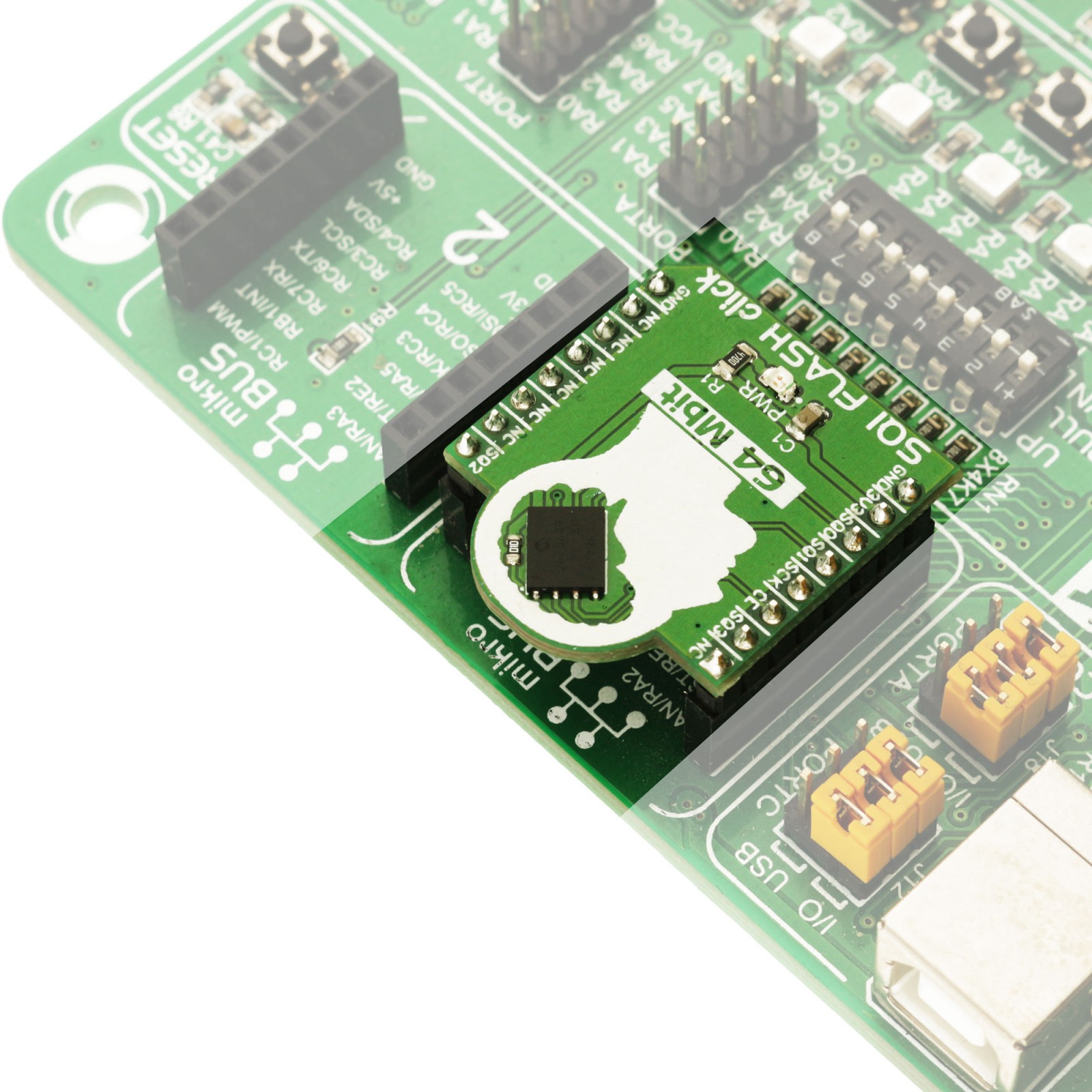
mikroBUS™
Click board size
S (28.6 x 25.4 mm)
Input Voltage
3.3V
Pinout diagram
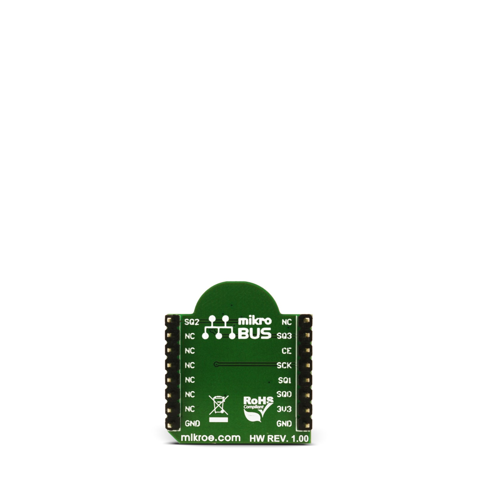
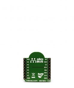
This table shows how the pinout on SQI FLASH click corresponds to the pinout on the mikroBUS™ socket (the latter shown in the two middle columns).
Note: When used in the SQI mode, some of the pins are used as additional data lines, as stated in front of the slash sign, in the table above. Otherwise, these pins have the functions as stated after the slash sign.
Onboard settings and indicators
| Label | Name | Default | Description |
|---|---|---|---|
| LD1 | PWR | – | Power LED indicator |
Software support
We provide an example for the SQI FLASH click on our LibStock page, as well as a demo application (example), developed using MikroElektronika compilers. The demo can run on all the main MikroElektronika development boards.
Library description
Library carries all the necessary functions for the SQI Flash click.
Key functions
void SQIFLASH_WriteArray(uint32_t address, uint8_t* pData, uint16_t number) – Writes array of data to the address specified
void SQIFLASH_ReadArray(uint32_t address, uint8_t* pData, uint16_t num) – Reads array of data from the address specified
void SQIFLASH_SectorErase(uint32_t address) – Erases sector where provided address belong to
Examples Description
The application is composed of three sections :
- System initialization – Initializes pins, SPI peripheral, UART used for logging.
- Application initialization – Initializes driver and configures module but also checks the communication by reading the chip ID.
- Application task – (Code snippet) Sequentially writes and reads data from the SQI FLASH click. Written and read data must match because both of them are at the same address. Information about the current reading and writing will be logged to UART.
The example uses the SQIFLASH_WriteByte function to write the value to a 32bit address, forwarded as the parameter to the write function. Both the value and the address are derived from the same variable – counter, which is increased at the end of the application task function. This value is printed at the UART terminal.
After that, SQIFLASH_ReadByte function is used to read from the address of the SQI Flash module and it is stored in a separate variable, labeled – result. This value gets converted and it gets printed at the UART terminal. The application task function is executed inside the while loop
void applicationTask()
{
    SQIFLASH_WriteByte(counter, counter);
    UART1_Write_Text( "rnValue Written : " );
    ByteToStr( counter, txt );
    UART1_Write_Text( txt );
    Delay_ms( 100 );

    result = SQIFLASH_ReadByte(counter);
    UART1_Write_Text( "rnValue Read : " );
    ByteToStr( result, txt );
    UART1_Write_Text( txt );
    Delay_ms( 100 );

    counter++;

    if (counter == 256)
    {
        counter = 0;
    }
    Delay_ms( 2000 );
}
The full application code, and ready to use projects can be found on our LibStock page.
Other mikroE Libraries used in the example:
- UART Conversions
Additional notes and information
Depending on the development board you are using, you may need USB UART click, USB UART 2 click or RS232 click to connect to your PC, for development systems with no UART to USB interface available on the board. The terminal available in all MikroElektronika compilers, or any other terminal application of your choice, can be used to read the message.
mikroSDK
This click board is supported with mikroSDK, the MikroElektronika Software Development Kit. To download mikroSDK visit LibStock. For more information about SDK, visit the official page.
Resources
Downloads
| Weight | 18 g |
|---|---|
| Brand | MikroElektronika |

