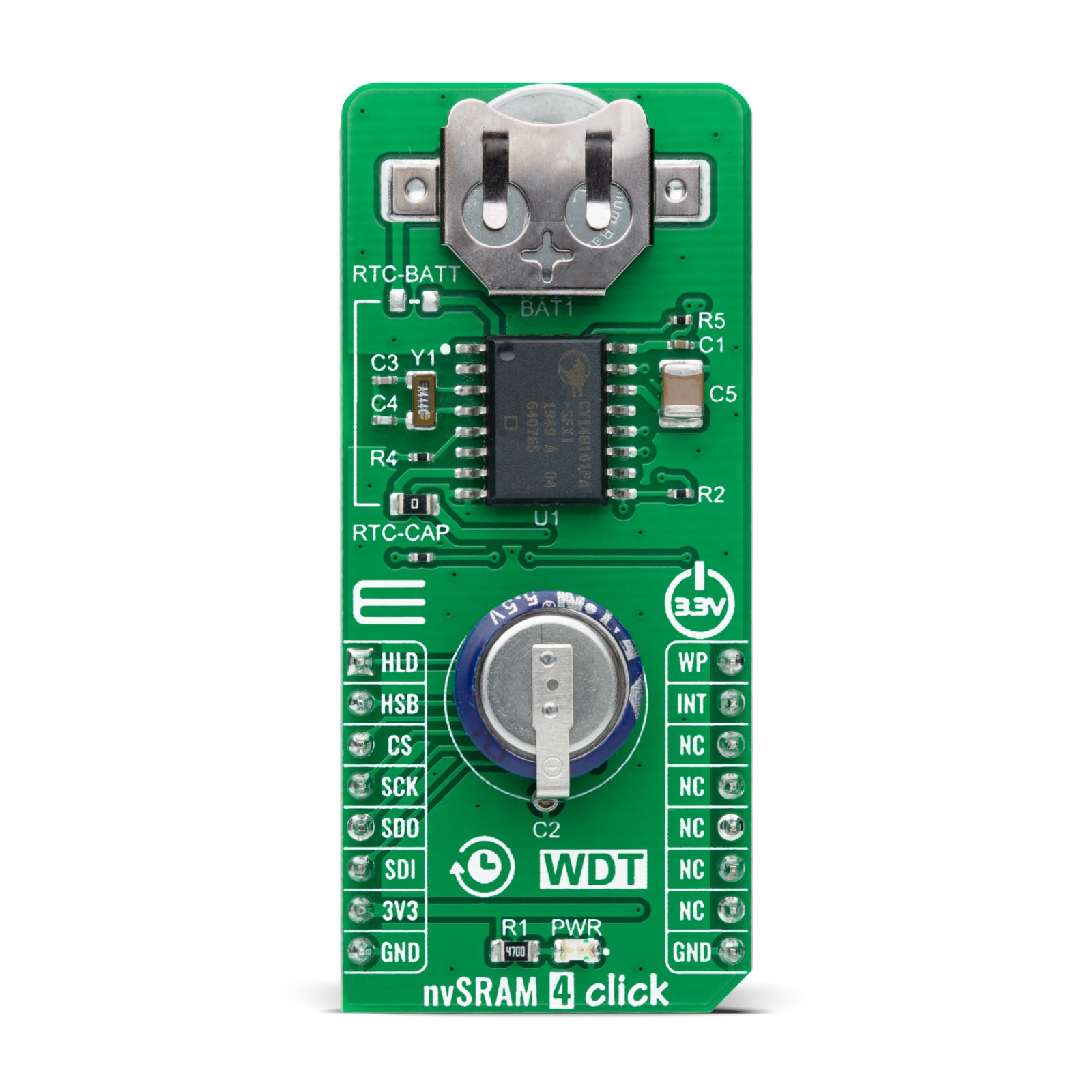
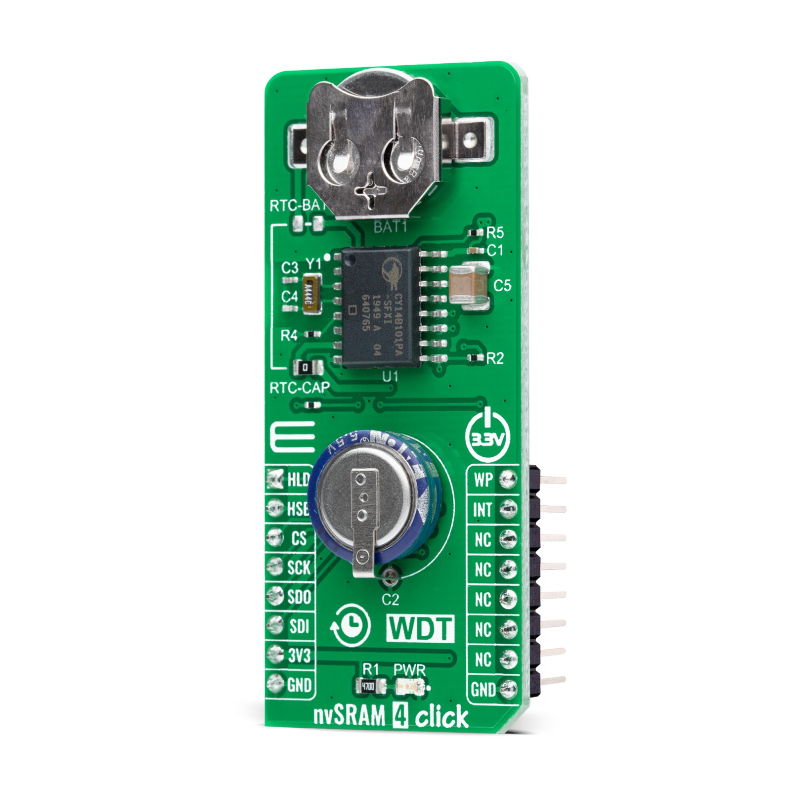
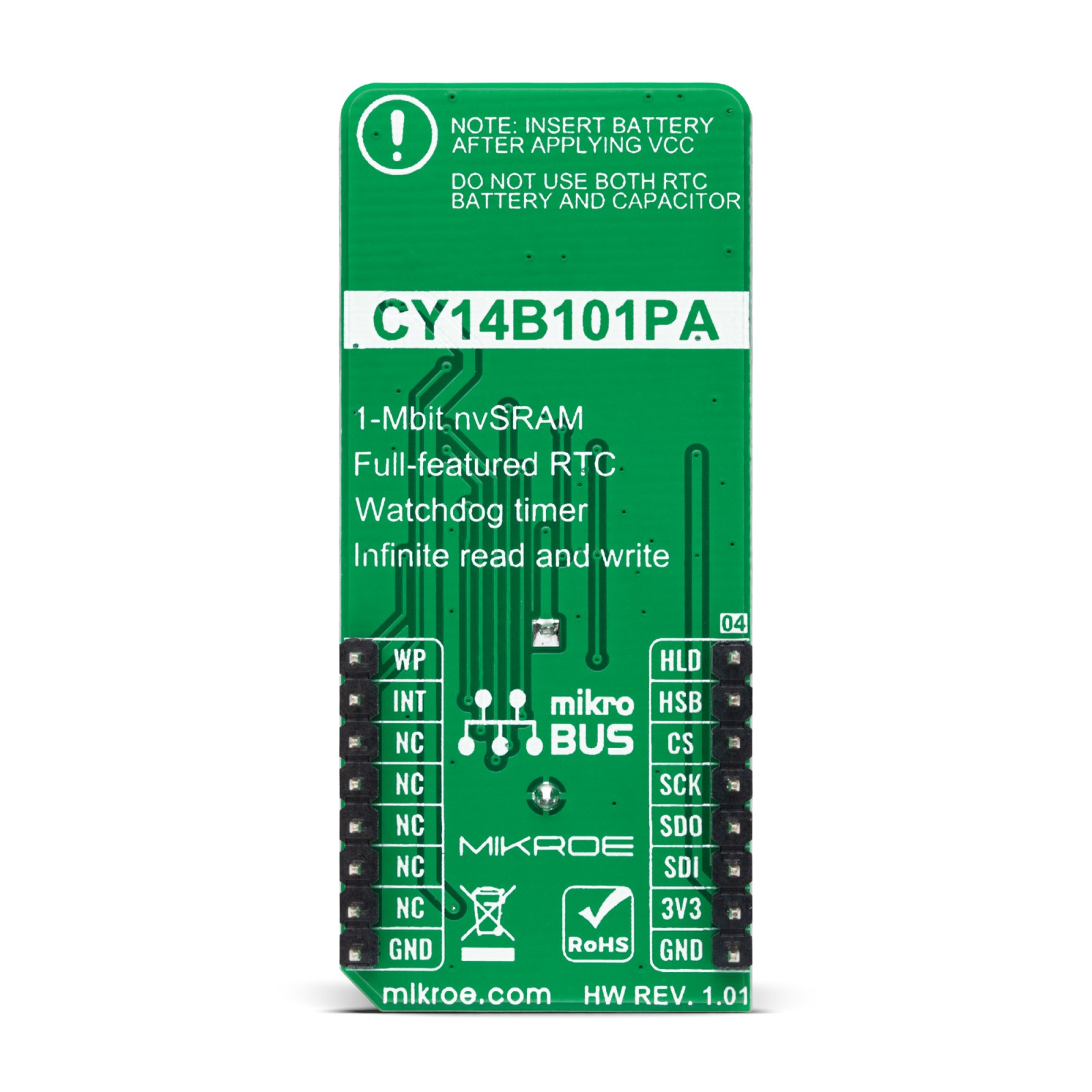
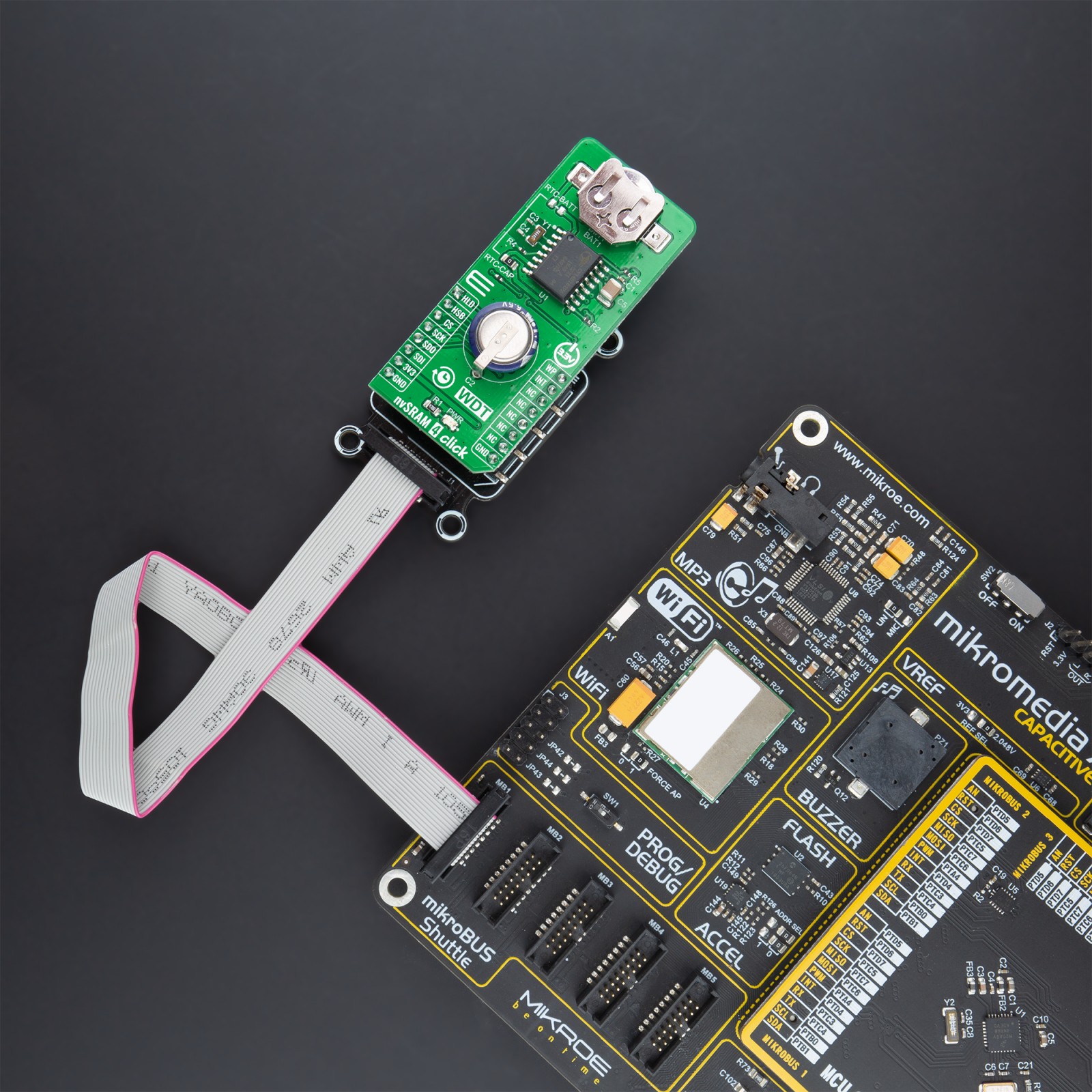
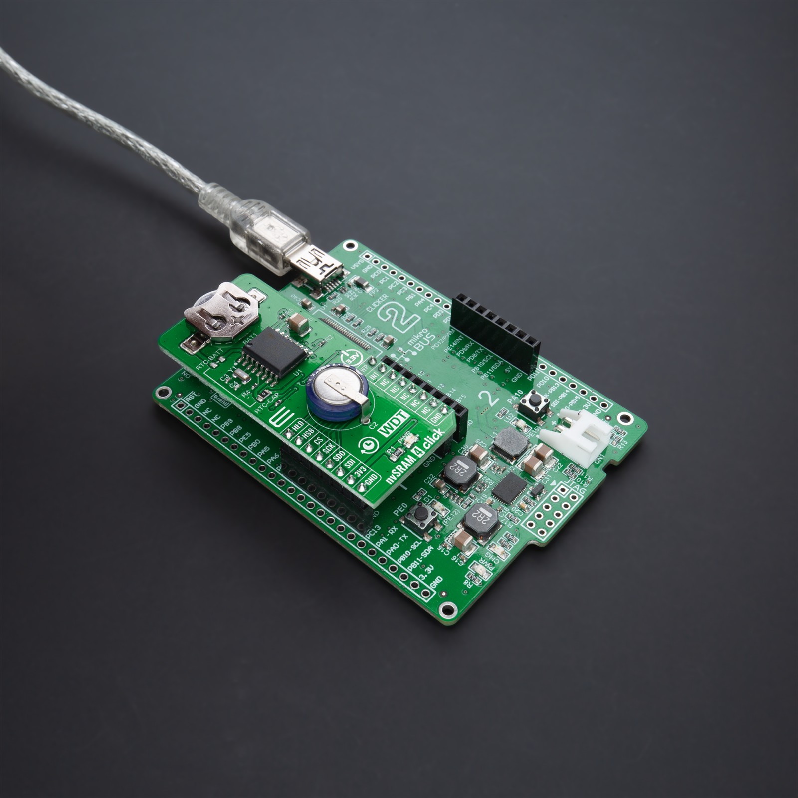
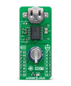
nvSRAM 4 Click
R770.00 ex. VAT
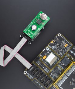
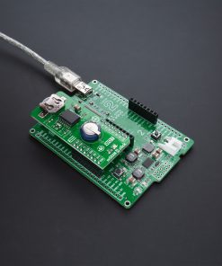
nvSRAM 4 Click is a compact add-on board that contains the most reliable nonvolatile memory. This board features the CY14B101PA, a 1-Mbit nvSRAM with a fully-featured real-time clock from Infineon. The memory is organized as 128K words of 8 bits each, where the embedded elements incorporate the QuantumTrap technology that provides highly reliable, nonvolatile data storage. It provides infinite read and writes cycles with an additional automatic backup switch. Data transfer, initiated by the user through SPI commands, takes place automatically at Power-Down. On the other hand, during the Power-Up, data is restored to the SRAM from the nonvolatile memory. This Click board™ is suitable for all applications that require fast access and high reliability of stored data, and unlimited endurance.
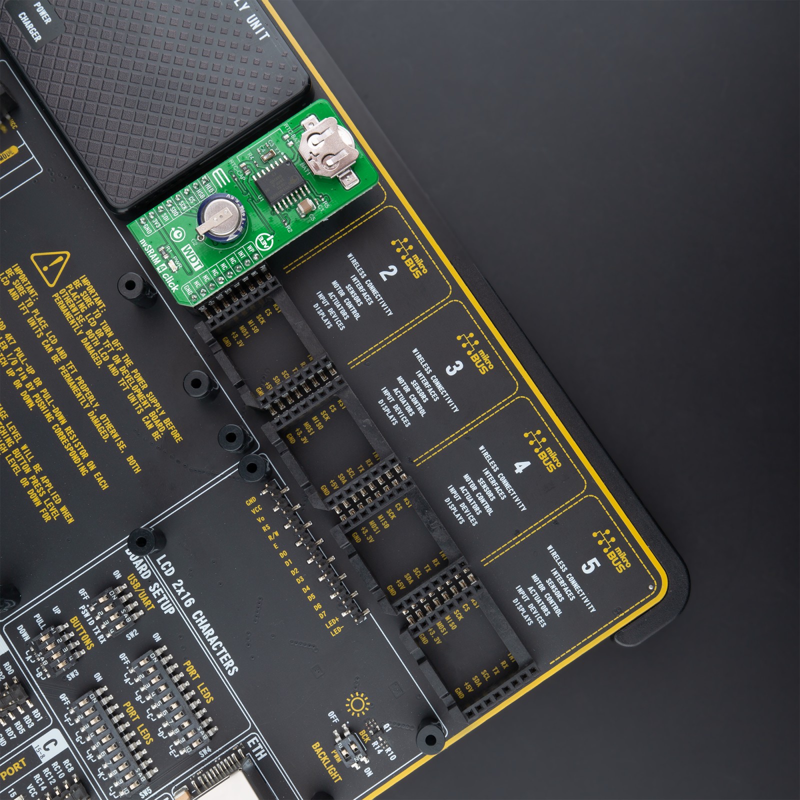
nvSRAM 4 Click is supported by a mikroSDK compliant library, which includes functions that simplify software development. This Click board™ comes as a fully tested product, ready to be used on a system equipped with the mikroBUS™ socket.
Stock: Lead-time applicable.
| 5+ | R731.50 |
| 10+ | R693.00 |
| 15+ | R654.50 |
| 20+ | R629.86 |
How does it work?
nvSRAM 4 Click is based on the CY14B101PA, a 1-Mbit nvSRAM memory organized as 128K words of 8 bits each, with a fully-featured real-time clock from Infineon. The nvSRAM specifies one million endurance cycles for nonvolatile cells with data retention of a minimum of 20 years. All the reads and writes to nvSRAM happen to the SRAM, which gives nvSRAM the unique capability to handle infinite writes to the memory. The benefit of nvSRAM over serial EEPROMs is that all reads and writes to nvSRAM are performed at the SPI speed with zero cycle delay, which means, therefore, no wait time is required after any of the memory accesses.

In addition to the CY14B101PA, this Click board™ is equipped with the button cell battery holder compatible with the 3000TR battery holder, suitable for 12mm Coin Cell batteries. When the primary power fails and drops below 2.65V, this Click board™ switches to the backup power supply by placing a jumper labeled as RTC-BATT. By utilizing an automatic backup, the CY14B101PA uses an external battery power source when there is no power supply on its main power terminals allowing for uninterrupted operation.
nvSRAM 4 Click communicates with MCU using a standard SPI interface with clock frequency up to 40MHz, zero cycle delay read, and write cycles. It also supports the two most common modes, SPI Mode 0 and 3, and 104 MHz SPI access speed with special instruction for the read operation. The CY14B101PA uses the standard SPI opcodes for memory access. In addition to the general SPI instructions for reading and writing, it provides four special instructions: STORE, RECALL, AutoStore Disable (ASDISB), and AutoStore Enable (ASENB).
The STORE operation of the CY14B101PA can be controlled and acknowledged via the HSB pin, routed on the RST pin of the mikroBUS™ socket. If no STORE/RECALL is in progress, this pin can be used to request a hardware STORE cycle. When the HSB pin is driven LOW, the CY14B101PA conditionally initiates a STORE operation. Also, this Click board™ can use the AutoStore feature of the SRAM data in nonvolatile cells when the power goes down, providing power-down data security by placing a jumper labeled as RTC-CAP.
An additional feature of this Click board™ represents the configurable Write Protection function labeled as WP routed on the PWM pin of the mikroBUS™ socket. The WP pin protects the entire memory and all registers from write operations and must be held high to inhibit all the write operations. When this pin is high, all memory and register writes are prohibited, and the address counter is not incremented. Besides, the nvSRAM 4 Click also has additional HOLD and Interrupt pins, routed to the AN and INT pins of the mikroBUS™ socket labeled as HLD and INT.
HLD pin is used to pause the serial communication without stopping the operation of write status register, programming, or erasing in progress. On the other hand, INT pin can be used in several ways such as interrupt output, calibration, or a square wave, programmable to respond to the clock alarm, the watchdog timer, and the power monitor.
This Click board™ is designed to be operated only with a 3.3V logic voltage level. A proper logic voltage level conversion should be performed before the Click board™ is used with MCUs with different logic levels. However, Mikroe equipped its users with a library that contains functions and an example code that can be used, as a reference, for further development.
Specifications
Type
SRAM
Applications
Can be used for all applications that require fast access and high reliability of stored data, and unlimited endurance.
On-board modules
CY14B101PA – 1-Mbit nvSRAM memory organized as 128K words of 8 bits each, with a fully-featured real-time clock from Cypress Semiconductor
Key Features
1Mbit nonvolatile static random access memory, high reliability, real-time clock, high speed interface, write protection, low power consumption, and more.
Interface
SPI
Feature
No ClickID
Compatibility
mikroBUS™
Click board size
L (57.15 x 25.4 mm)
Input Voltage
3.3V
Pinout diagram
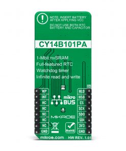
This table shows how the pinout on nvSRAM 4 Click corresponds to the pinout on the mikroBUS™ socket (the latter shown in the two middle columns).
Onboard settings and indicators
| Label | Name | Default | Description |
|---|---|---|---|
| LD1 | PWR | – | Power LED Indicator |
| JP1 | RTC-BATT | Unpopulated | RTC Battery Backup Selection |
| JP2 | RTC-CAP | Populated | RTC Capacitor Backup Selection |
nvSRAM 4 Click electrical specifications
| Description | Min | Typ | Max | Unit |
|---|---|---|---|---|
| Supply Voltage | – | 3.3 | – | V |
| Battery Backup Supply Voltage | 1.8 | 3 | 3.6 | V |
| Memory Size | – | – | 1 | Mbit |
| nvSRAM Write Endurance | 1000000 | – | – | Write Cycles |
| nvSRAM Data Retention | 20 | – | – | Years |
| Operating Temperature Range | -40 | +25 | +85 | °C |
Software Support
We provide a library for the nvSRAM 4 Click as well as a demo application (example), developed using MikroElektronika compilers. The demo can run on all the main MikroElektronika development boards.
Package can be downloaded/installed directly from NECTO Studio Package Manager(recommended way), downloaded from our LibStock™ or found on mikroE github account.
Library Description
This library contains API for nvSRAM4 Click driver.
Key functions:
void nvsram4_cfg_setup ( nvsram4_cfg_t *cfg );– Config Object Initialization function.NVSRAM4_RETVAL nvsram4_init ( nvsram4_t *ctx, nvsram4_cfg_t *cfg );– Initialization function.void nvsram4_default_cfg ( nvsram4_t *ctx );– Click Default Configuration function.
Examples description
This is an example that demonstrates the use of the nvSRAM 4 Click board™.
The demo application is composed of two sections :
void application_task ( void ) {
    nvsram4_get_rtc_time( &nvsram4, &time );
    Delay_ms( 1 );
    nvsram4_get_rtc_date( &nvsram4, &date );
    Delay_ms( 1 );

    if ( time.sec != new_sec ) {
        log_printf( &logger, "  Date      : %.2d-%.2d-%.2drn", ( uint16_t ) date.day, ( uint16_t ) date.month, ( uint16_t ) date.year );
        log_printf( &logger, "  Time      : %.2d:%.2d:%.2drn", ( uint16_t ) time.hours, ( uint16_t ) time.min, ( uint16_t ) time.sec );
        log_printf( &logger, "- - - - - - - - - - - -rn" );
        new_sec = time.sec;
        Delay_ms( 10 );

        if ( date.year != c_year ) {
            log_printf( &logger, "     Happy New Year    rn" );
            c_year = date.year;
            Delay_ms( 10 );
        } else {
            nvsram4_burst_read_memory( &nvsram4, memory_addr, &rx_data[ 0 ], 9 );
            log_printf( &logger, "  Read data : %s", rx_data );
        }

        log_printf( &logger, "-----------------------rn" );
    } else {
        Delay_ms( 1 );
    }
}
The full application code, and ready to use projects can be installed directly from NECTO Studio Package Manager(recommended way), downloaded from our LibStock™ or found on mikroE github account.
Other mikroE Libraries used in the example:
- MikroSDK.Board
- MikroSDK.Log
- Click.nvSRAM4
Additional notes and informations
Depending on the development board you are using, you may need USB UART click, USB UART 2 click or RS232 click to connect to your PC, for development systems with no UART to USB interface available on the board. The terminal available in all MikroElektronika compilers, or any other terminal application of your choice, can be used to read the message.
mikroSDK
This Click board™ is supported with mikroSDK – MikroElektronika Software Development Kit. To ensure proper operation of mikroSDK compliant Click board™ demo applications, mikroSDK should be downloaded from the LibStock and installed for the compiler you are using.
For more information about mikroSDK, visit the official page.
Resources
Downloads
| Weight | 22 g |
|---|---|
| Brand | MikroElektronika |

