How does it work?
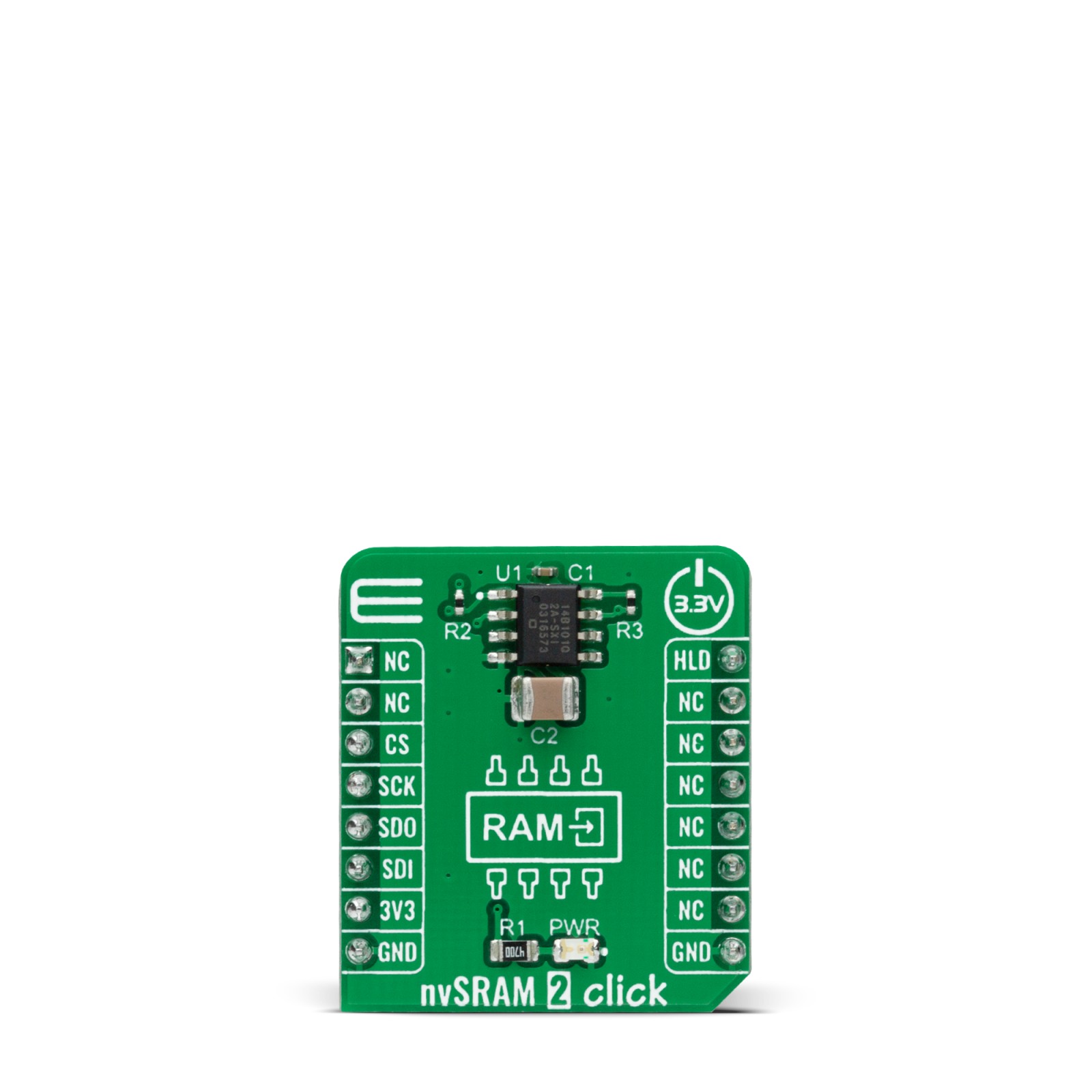
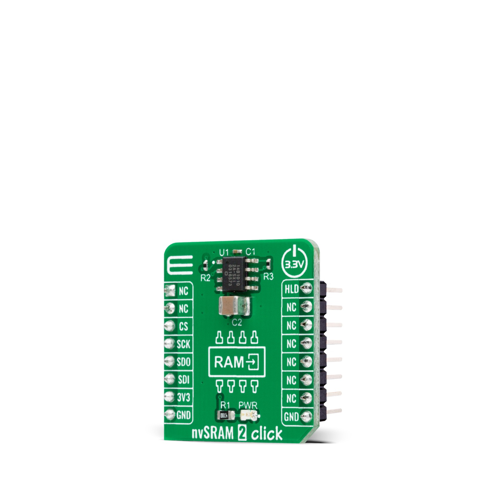
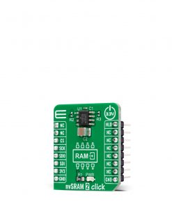
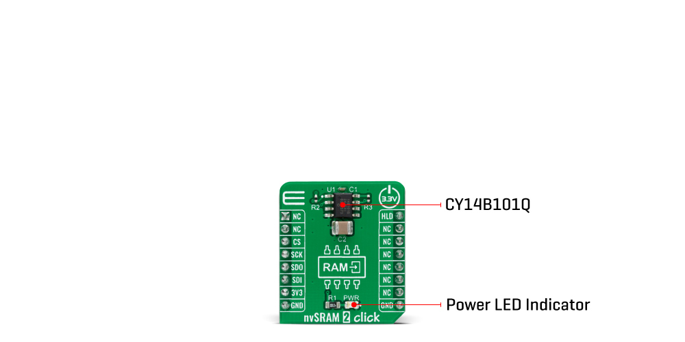
nvSRAM 2 Click is based on the CY14B101Q, a 1-Mbit nvSRAM organized as 128K words of 8 bits each with a nonvolatile element in each memory cell from Infineon. The nvSRAM specifies one million endurance cycles for nonvolatile cells with data retention of a minimum of 20 years. All the reads and writes to nvSRAM happen to the SRAM, which gives nvSRAM the unique capability to handle infinite writes to the memory. Besides, the benefit of nvSRAM over serial EEPROMs is that all reads and writes to nvSRAM are performed at the SPI speed with zero cycle delay. Therefore, no wait time is required after any of the memory accesses.
In the event of system power loss, data from the SRAM is transferred to its nonvolatile cell automatically by using energy stored in a capacitor labeled as C2. During the Power-Up, data from the nonvolatile cell is recalled automatically in the SRAM array and available to the user. The endurance cycle is consumed only when data transfer happens from the SRAM cells to nonvolatile cells during the Power-Down.
The memory can be accessed through a standard SPI interface that enables high clock speeds up to 40 MHz with zero cycle delay read and write cycles. It also supports the two most common modes, SPI Mode 0 and 3, and 104 MHz SPI access speed with special instruction for the read operation. The CY14B101Q uses the standard SPI opcodes for memory access. In addition to the general SPI instructions for reading and writing, it provides four special instructions: STORE, RECALL, AutoStore Disable (ASDISB), and AutoStore Enable (ASENB).
In addition to this, the nvSRAM 2 Click also has an additional HOLD pin, routed to the PWM pin of the mikroBUS™ socket labeled as HLD, used to pause the serial communication with the device without having to stop the operation of write status register, programming, or erasing in progress.
This Click board™ is designed to be operated only with a 3.3V logic voltage level. A proper logic voltage level conversion should be performed before the Click board™ is used with MCUs with different logic levels.
Specifications
Type
SRAM
Applications
Can be used for all applications that require fast access and high reliability of stored data, and unlimited endurance.
On-board modules
nvSRAM 2 Click is based on the CY14B101Q, a 1-Mbit nvSRAM organized as 128K words of 8 bits each with a nonvolatile element in each memory cell from Cypress Semiconductor.
Key Features
Low power consumption, 1Mbit nonvolatile static random access memory, high reliability, high speed interface, write protection feature, and more.
Interface
SPI
Feature
No ClickID
Compatibility
mikroBUS™
Click board size
S (28.6 x 25.4 mm)
Input Voltage
3.3V
Pinout diagram
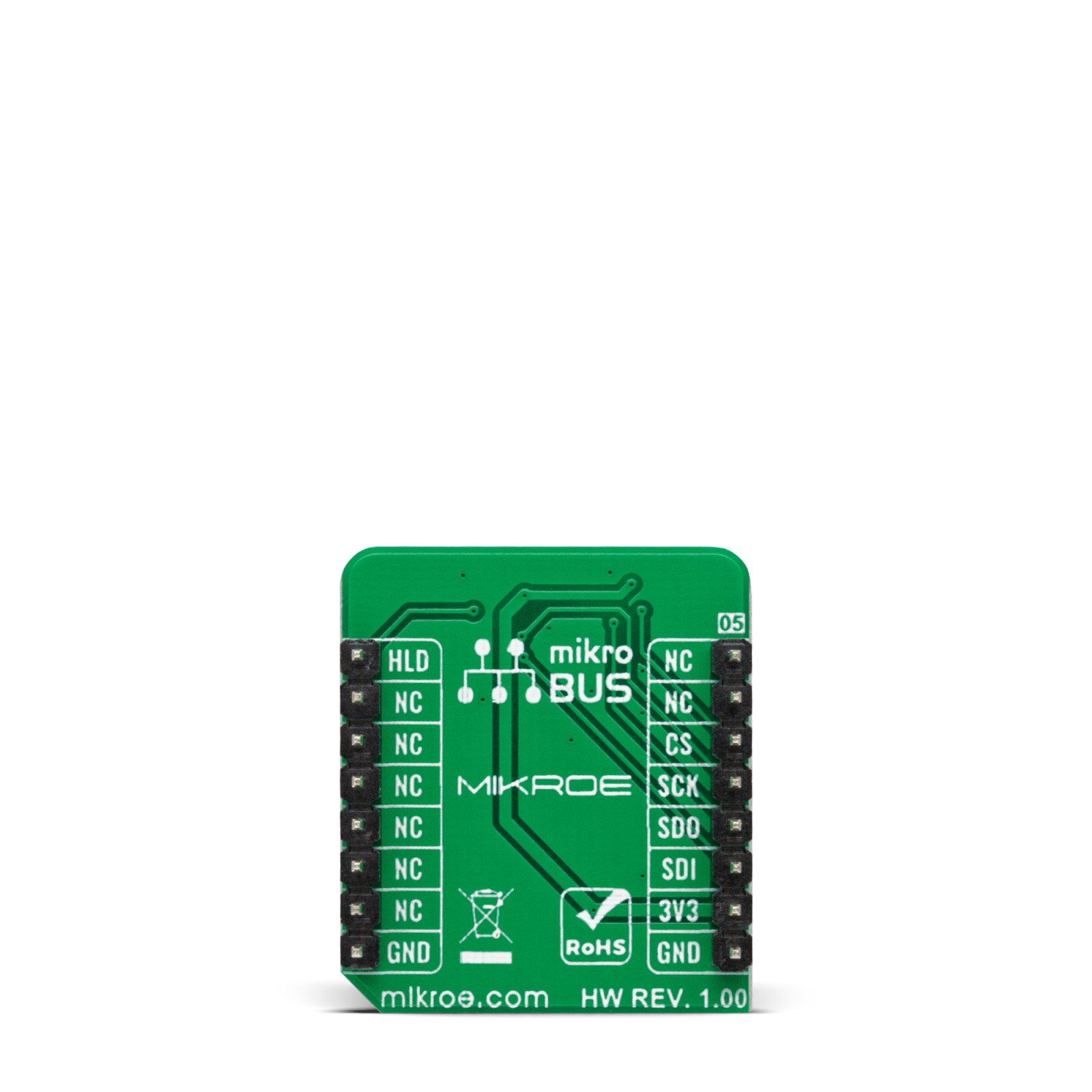
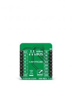
This table shows how the pinout on nvSRAM 2 Click corresponds to the pinout on the mikroBUS™ socket (the latter shown in the two middle columns).
Onboard settings and indicators
Label | Name | Default | Description |
---|---|---|---|
LD1 | PWR | – | Power LED Indicator |
nvSRAM 2 Click electrical specifications
Description | Min | Typ | Max | Unit |
---|---|---|---|---|
Supply Voltage | -0.5 | 3.3 | 4.1 | V |
Memory Size | – | – | 1 | Mbit |
nvSRAM Write Endurance | 1.000.000 | – | – | Write Cycles |
nvSRAM Data Retention | 20 | – | – | Years |
Operating Temperature Range | -40 | – | +85 | °C |
Software Support
We provide a library for the nvSRAM 2 Click on our LibStock page, as well as a demo application (example), developed using MikroElektronika compilers. The demo can run on all the main MikroElektronika development boards.
Library Description
The library covers all the necessary functions to control nvSRAM 2 Click board™. Library performs a standard SPI interface communication.
Key functions:
void nvsram2_set_cmd ( uint8_t cmd )
– Set command function.void nvsram2_burst_write ( uint32_t mem_addr, uint8_t *p_tx_data, uint8_t n_bytes );
– Burst write function.void nvsram2_burst_read ( uint32_t mem_addr, uint8_t *p_rx_data, uint8_t n_bytes );
– Burst read function.
Examples description
The application is composed of three sections :
- System Initialization – Initializes SPI and UART LOG, sets CS and PWM pins as outputs.
- Application Initialization – Initialization driver enables SPI, disables hold, sets write enable latch, targets the memory address at 12345 ( 0x00003039 ) for burst write starting point and writes data which is also displayed on the log.
- Application Task – This is an example that demonstrates the use of the nvSRAM 2 Click board™. In this example, the data is read from the targeted memory address. The results are being sent to the Usart Terminal. This task repeats every 5 sec.
void application_task ( ) { mikrobus_logWrite( "-----------------------", _LOG_LINE ); mikrobus_logWrite( "", _LOG_LINE ); mikrobus_logWrite( "<- Read data : ", _LOG_TEXT ); nvsram2_burst_read( memory_addr, &rx_data[ 0 ], 9 ); mikrobus_logWrite( rx_data, _LOG_LINE ); Delay_ms( 5000 ); }
The full application code, and ready to use projects can be found on our LibStock page.
Other mikroE Libraries used in the example:
- SPI
- UART
Additional notes and informations
Depending on the development board you are using, you may need USB UART click, USB UART 2 click or RS232 click to connect to your PC, for development systems with no UART to USB interface available on the board. The terminal available in all MikroElektronika compilers, or any other terminal application of your choice, can be used to read the message.
mikroSDK
This Click board™ is supported with mikroSDK – MikroElektronika Software Development Kit. To ensure proper operation of mikroSDK compliant Click board™ demo applications, mikroSDK should be downloaded from the LibStock and installed for the compiler you are using.
For more information about mikroSDK, visit the official page.