MRAM Click
R410.00 ex. VAT
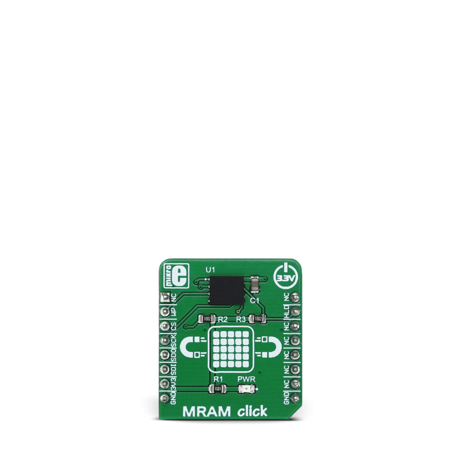
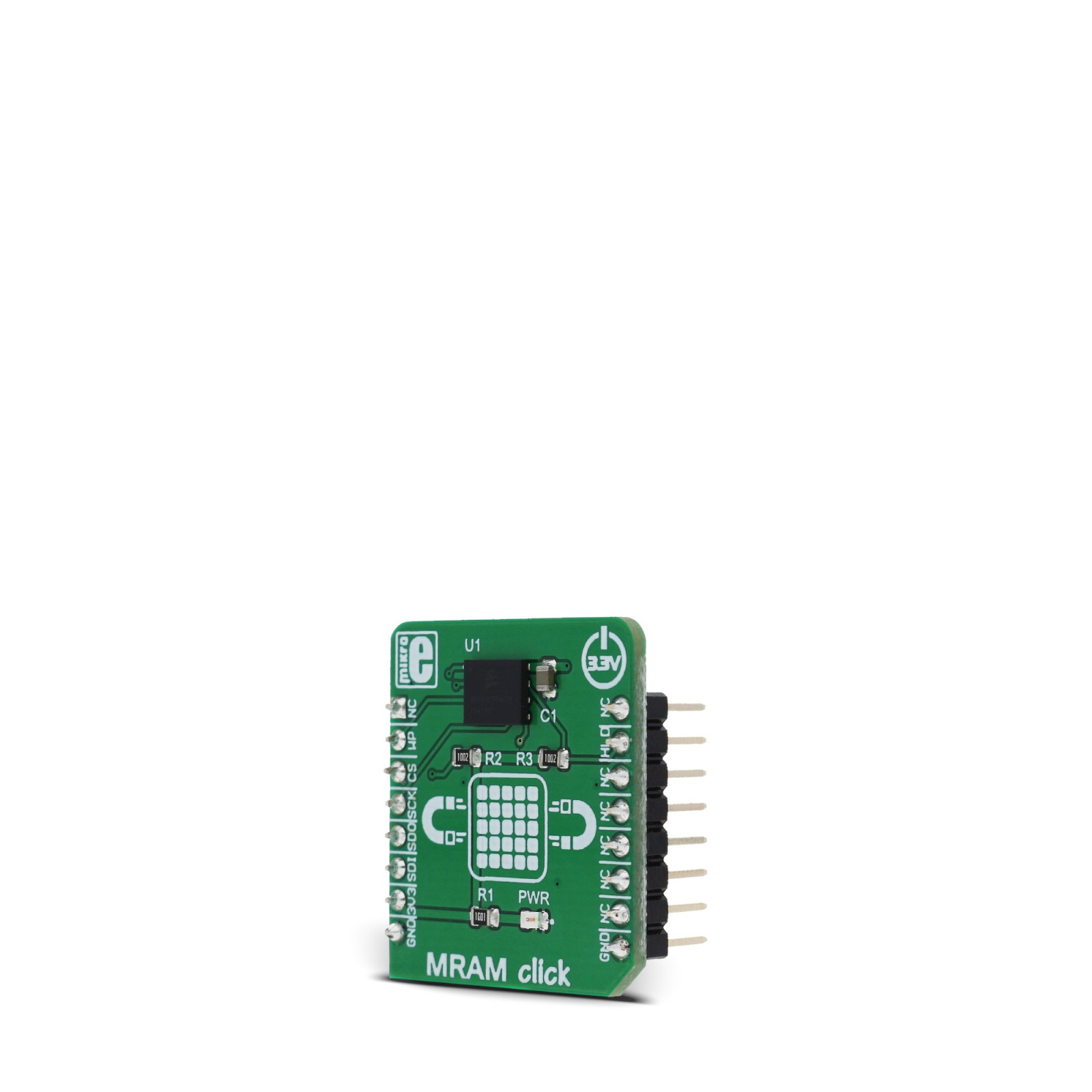
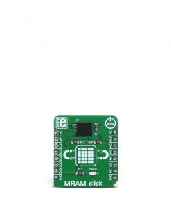
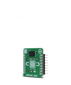
MRAM click features MRAM module which contains 262,144 magnetoresistive memory cells, organized into 32,768 bytes of memory. It means that MRAM click is a memory storage device with 32KB of memory space. The used memory module can withstand an unlimited number of write cycles, it has data retention period greater than 20 years and it can read and write to random addresses with no delay.
Besides these features that already mark this kind of memory modules a milestone in memory manufacturing technology, the device features data protection in case of power loss, block write protection, low power consumption and fast SPI interface that can theoretically work up to 40MHz. Because of its universal memory characteristics, MRAM click can be used both as a non-volatile storage media, or temporary RAM expansion for storing variables in any embedded application.
Stock: Lead-time applicable.
| 5+ | R389.50 |
| 10+ | R369.00 |
| 15+ | R348.50 |
| 20+ | R335.38 |
MRAM click features MRAM module which contains 262,144 magnetoresistive memory cells, organized into 32,768 bytes of memory. It means that MRAM click is a memory storage device with 32KB of memory space. The used memory module can withstand an unlimited number of write cycles, it has data retention period greater than 20 years and it can read and write to random addresses with no delay.
Besides these features that already mark this kind of memory modules a milestone in memory manufacturing technology, the device features data protection in case of power loss, block write protection, low power consumption and fast SPI interface that can theoretically work up to 40MHz. Because of its universal memory characteristics, MRAM click can be used both as a non-volatile storage media, or temporary RAM expansion for storing variables in any embedded application.
How does it work?
MRAM is an abbreviation for Magnetoresistive Random Access Memory. This is a fairly new type of memory, first introduced in the ’90s. The main features of MRAM modules include unlimited write endurance, read and write cycles with no delay and data retention even after power loss. This makes these modules a kind of universal memory, a hybrid between standard RAM modules and EEPROM and similar types of FLASH memory. The ability to randomly access the memory cells without the need to refresh them and with no delay makes this type of memory looks like an SRAM. Data retention after power off, makes it look like a FLASH memory. Therefore, it is often referred to as the Universal memory.
There are certain downsides and flaws that prevent this type of memory to become the main memory medium and replace all types of memory used so far. It is the cell density achievable with this technology. Unlike the memory modules used so far which store data as the electrical charge, this type of memory uses magnetic elements to store data. Two plates are used – one is a permanent magnet, while the other plate can be magnetized by a current flow through the conductors and the resulting induced magnetic field. The problem with this is obvious: it is impossible to contain the induced magnetic field in a space small enough to allow for very high cell densities. There are various methods used to overcome this problem, but it remains the main reason why this type of memory hasn’t replaced other memory types, yet. However, in the embedded world, where the memory amount demands are rather limited, this type of memory most certainly deserves attention.
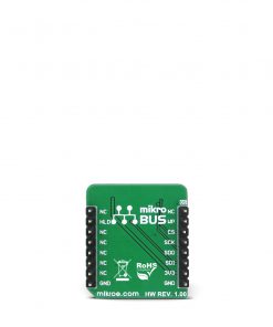
MRAM click board uses the MR25H256, a 256 kilobits serial SPI MRAM memory module from Everspin company. This module contains 262,144 bits of memory that can be randomly accessed. The pinout of the used memory module is the same as most commonly used EEPROM modules so that it can directly replace it. The usual SPI lines – SO, SI, SCK and #CS pins from the MR25H256 IC are routed to the mikroBUS™ SPI port (MISO, MOSI, SCK and CS pins). Besides the SPI serial bus, there are two more pins routed to the mikroBUS™.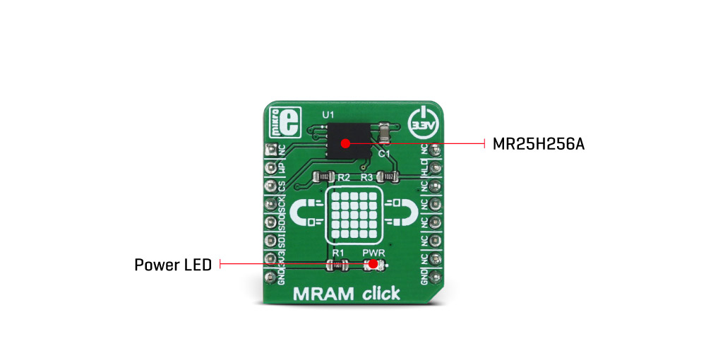
The #HOLD pin of the MR25H256 IC is routed to the INT pin of the mikroBUS™ and it is used to hold the data transfer. When this pin is pulled to a LOW logic level, all data transfer operations are suspended. However, this function is enabled only when the device is already addressed with the CS pin pulled to a LOW level. This allows to pause the data transfer and resume it later without the need to first address it via the CS pin, reducing the output latency that way. While the data transfer is paused, the SO pin will switch to a high impedance mode (HIGH Z) and will remain inactive. The SCK pulses are completely ignored. The #HOLD pin of the MR25H256 IC is pulled to a HIGH logic level by an onboard pull-up resistor.
The #WP pin of the MR25H256 IC is routed to the INT pin of the mikroBUS™ and it is used to prevent writes to the status register, acting as a hardware write protect pin. It is routed to the RST pin of the mikroBUS™.
The logical organization of the moduke, such as read and write commands and the status register of the MR25H256 IC are the same as with most commonly used EEPROM modules, such as the one used in EEPROM 4 click. That allows this memory module, as well as MRAM click to replace the existing EEPROM module with not too much additional work. The provided libraries offer all the functions needed to work with the MRAM click. Their usage is demonstrated in the included example application which can be used as a reference for further development. The device should wait for the system voltage to become stable before the writing is attempted. The table below contains write inhibit voltage threshold, as well as the startup time that has to expire for the device to become fully operational. The board is powered only by the 3.3V rail of the mikroBUS™.
Specifications
Type
MRAM
Applications
The MRAM click can be used for any application that requires fast and reliable nonvolatile storage media. Due to its speed and unlimited endurance, it can be used as a temporary storage for the application runtime data operations
On-board modules
MR25H256A, a magnetoresistive random access memory (MRAM) device with 262,144 bits, organized as 32,768 of 8bit words
Key Features
MRAM click features an MRAM memory module. Due to the used memory type, it inherits all the benefits of having both features typically found RAM and EEPROM modules. Fast, nonvolatile memory which can endure an unlimited number of write cycles
Interface
GPIO,SPI
Feature
No ClickID
Compatibility
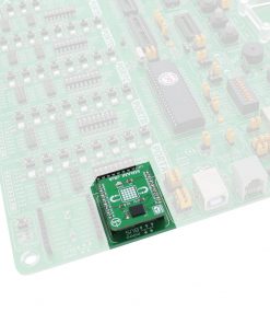
mikroBUS™
Click board size
S (28.6 x 25.4 mm)
Input Voltage
3.3V
Pinout diagram
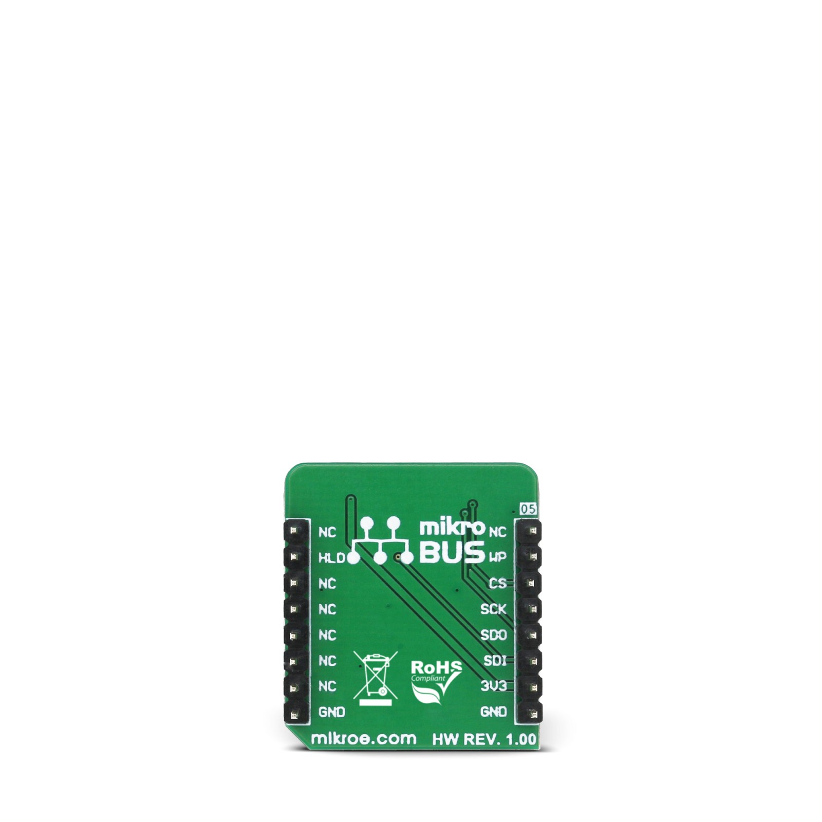
This table shows how the pinout on MRAM click corresponds to the pinout on the mikroBUS™ socket (the latter shown in the two middle columns).
MRAM click electrical specifications
| Description | Min | Typ | Max | Unit |
|---|---|---|---|---|
| SCK Clock Frequency | 0 | 40 | MHz | |
| Write Inhibit Voltage Threshold | 2.2 | 2.7 | V | |
| Startup timer | 400 | uS |
Onboard settings and indicators
| Label | Name | Default | Description |
|---|---|---|---|
| LD1 | Power LED | – | Power LED indicator |
Software support
We provide a library for MRAM click on our LibStock page, as well as a demo application (example), developed using MikroElektronika compilers and mikroSDK. The provided click library is mikroSDK standard compliant. The demo application can run on all the main MikroElektronika development boards.
Library Description
Initializes and defines SPI bus driver and driver functions which are used for storing data to memory and for reading memory.
Library also communicates with the Status register. For more details check the documentation.
Key functions
uint8_t mram_checkStatusBit(uint8_t status_bit)– The function checks one bit from the Status register determined by the function parameter.
void mram_readDataBytes(const uint16_t address, uint8_t *buffer, const uint16_t nBytes)– The function reads a number of bytes determined by the nBytes parameter from the memory to the buffer with start address determined by the address parameter.
void mram_writeDataBytes(const uint16_t address, uint8_t *buffer, const uint16_t nBytes)– The function writes a number of bytes determined by the nBytes parameter from the buffer to memory with start address determined by address parameter.
void mram_enableHoldMode(uint8_t state)– A low on the Hold pin interrupts a memory operation for another task.
Examples Description
The application is composed of three sections :
- System Initialization – Initializes peripherals and pins.
- Application Initialization – Initializes click driver.
- Application Task – Writes 6 bytes of buffer data in the memory with start address 0x0000. Then reads 3 bytes from the memory with start address 0x0002 and shows the result on USB UART.
void applicationTask()
{
    uint8_t numberBytesWrite;
    uint8_t numberBytesRead;
    char txt[20] = {0};
    uint16_t i;

    numberBytesWrite = 6;
    numberBytesRead = 3;

    mram_writeDataBytes(0x0000, &data_write[0], numberBytesWrite);

    mram_readDataBytes(0x0002, &data_read[0], numberBytesRead);

    for(i = 0; i < numberBytesRead; i++)
    {
        WordToStr(data_read[i], txt);
        mikrobus_logWrite(txt, _LOG_LINE);
    }

    Delay_ms(2000);
}
The full application code, and ready to use projects can be found on our LibStock page.
Additional notes and information
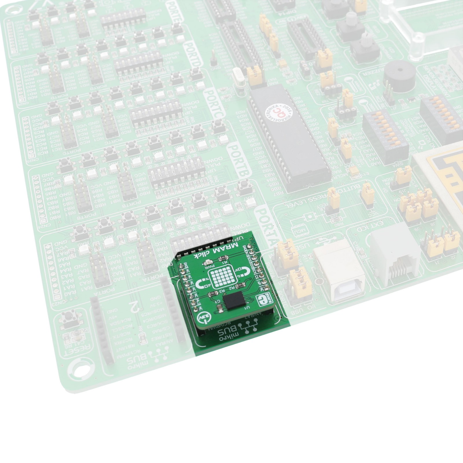
Depending on the development board you are using, you may need USB UART click, USB UART 2 click or RS232 click to connect to your PC, for development systems with no UART to USB interface available on the board. The terminal available in all MikroElektronika compilers, or any other terminal application of your choice, can be used to read the message.
mikroSDK
This click board is supported with mikroSDK - MikroElektronika Software Development Kit. To ensure proper operation of mikroSDK compliant click board demo applications, mikroSDK should be downloaded from the LibStock and installed for the compiler you are using.
For more information about mikroSDK, visit the official page.
Resources
Downloads
| Weight | 17 g |
|---|---|
| Brand | MikroElektronika |

