How does it work?
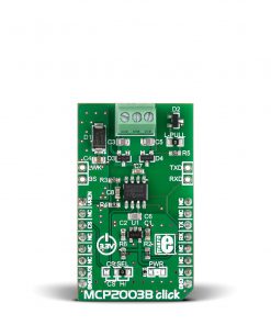
MCP2003B Click is based on the MCP2003B, a LIN transceiver from Microchip. This transceiver has both short-circuit and overtemperature protection by internal circuitry. It is designed to operate in an automotive environment and will work in specified transient conditions while meeting all stringent quiescent requirements. The MCP2003B has very high electromagnetic immunity (EMI), 60V load dump protection, high electrostatic discharge (ESD) immunity without TVS, and very high immunity to RF disturbances. It also can work in low-power mode and has an automatic thermal shutdown. One of the protections is direct capacitor coupling robustness without transient voltage suppressor (TVS) of ±35V and ±85V on LBUS, ground loss protection, reverse supply protection and many more.
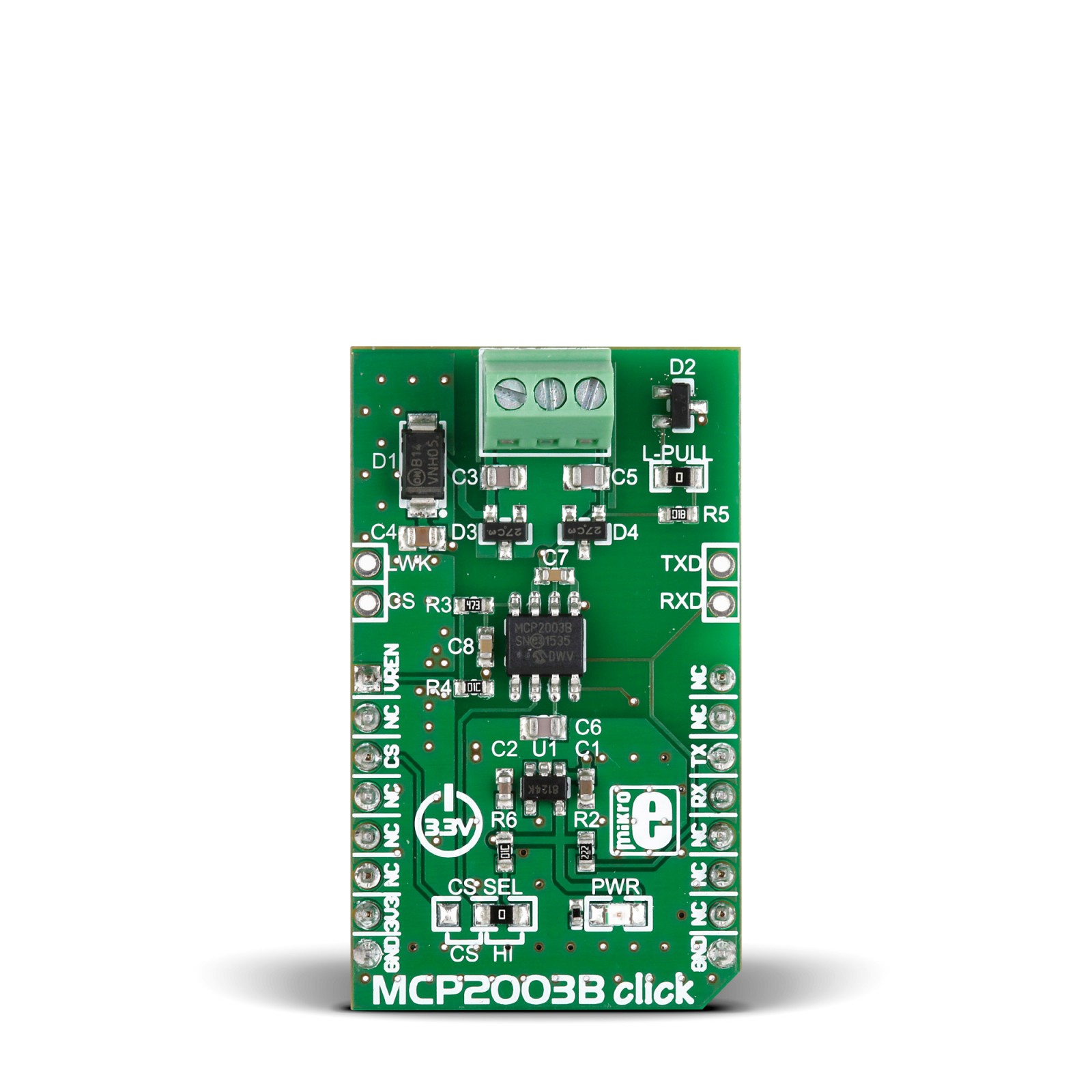
The MCP2003B Click has four operational modes: Power-Down mode, Ready mode, Operation mode, and Transmitter OFF mode. In Power-Down mode, the lowest power mode, everything except the wake-up pin (LWK on an unpopulated header) is shut down. LIN Bus activity typically changes the device from Power-down to Ready mode in 70μs. In Ready mode, the receiver is powered up and is ready to receive data while the transmitter is disabled. In Operational mode, all internal modules are operational. The Transmitter OFF mode is reached whenever the transmitter is disabled due to a fault condition, for example, if there is a thermal overload, bus contention, RSD monitoring, and TXD timer expiration. For the typical application as a Master node, the MCP2003B requires the LBUS line of the chip to be connected to the VBB of the LIN BUS, achievable via a populated L-PULL jumper. This jumper can be removed in other scenarios, such as the LIN Slave node.
To communicate with the host microcontroller, the MCP2003B uses a UART interface with commonly used UART RX and TX pins as its default communication protocol to transmit and exchange data. The RX pin is internally monitored and must be at a high level, while LBUS is recessive in Operation mode. Otherwise, an internal fault will be created, and the device will transition to Transmitter Off mode. A voltage regulator sensing circuit, comprised of an MCP1804 regulator and controlled via MCP2003B itself, is connected to the RX pin and internally monitors the RX pin when the LBUS line is recessive (RX is in a high logic state). If the RX pin is left open, it will not allow the device to switch (or stay) in Operation Mode. That’s why the RX pin is connected to a valid supply, provided by the voltage regulator, through a pull-up 2.2kΩ resistor.
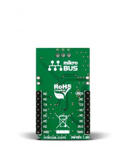
A CS SEL jumper can be used to set the chip select pin of the MCP2003B permanently connected to a logic HIGH (set by default), thus enabled all the time, or that the MCU performs this function via the CS of the mikroBUS™ socket. The extra pins LWK (CS on mikroBUS™ socket), CS (Wake-up pin on MCP2003B), TX, and RX are also available above the mikroBUS™ and can be used for external control. The wake-up from power-down mode can be controlled only through the LWK pin of this header. The RXD, TXD, CS, and LWK pins tolerate high voltage.
This Click board™ can be operated only with a 3.3V logic voltage level. The board must perform appropriate logic voltage level conversion before using MCUs with different logic levels. However, the Click board™ comes equipped with a library containing functions and an example code that can be used, as a reference, for further development.
Specifications
Type
LIN
Applications
Can be used for the development of sensor networks for vehicles
On-board modules
MCP2003B – LIN transceiver from Microchip
Key Features
Bi-directional LIN transceiver, LIN BUS interface tolerant to high voltages, supported baud rates of up to 20Kbaud, very high electromagnetic immunity (EMI), high electrostatic discharge (ESD), wide supply voltage, low power mode, automatic thermal shutdown, and more
Interface
GPIO,UART
Feature
No ClickID
Compatibility
mikroBUS™
Click board size
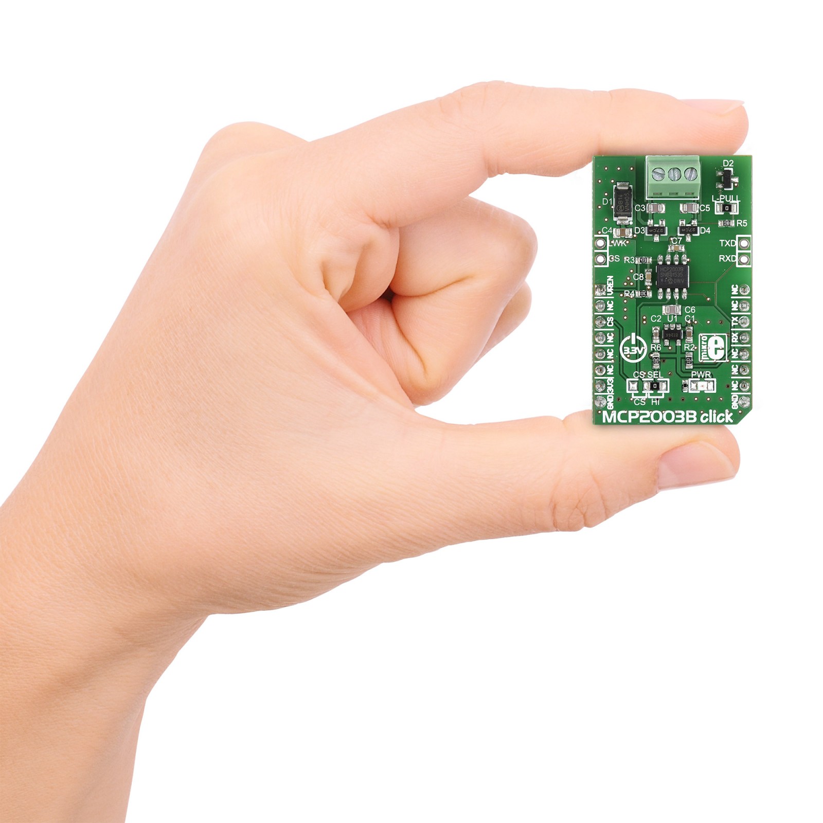
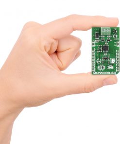
M (42.9 x 25.4 mm)
Input Voltage
3.3V
Pinout diagram
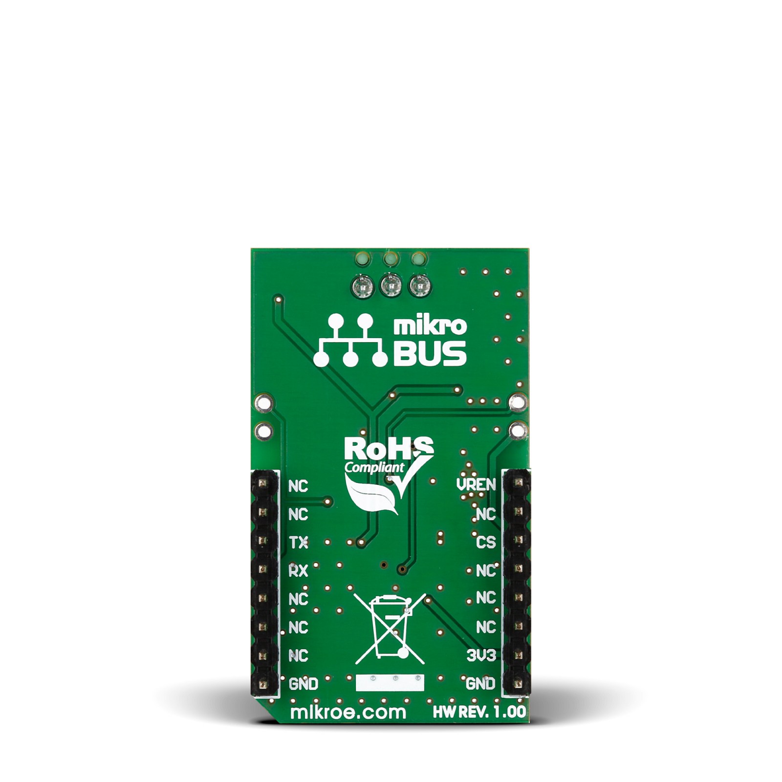
This table shows how the pinout on MCP2003B Click corresponds to the pinout on the mikroBUS™ socket (the latter shown in the two middle columns).
Onboard settings and indicators
Label | Name | Default | Description |
---|---|---|---|
– | PWR | – | Power LED Indicator |
J1 | CS SEL | Right | Chip Select Selection CS/HI: Left position CS, Right position HI |
JMPR | L-PULL | Populated | Master Node Operation Selection Jumper |
MCP2003B Click electrical specifications
Description | Min | Typ | Max | Unit |
---|---|---|---|---|
Supply Voltage | – | 3.3 | – | V |
LIN Supply Voltage | 5.5 | – | 30 | V |
Load Dump Protection | – | 60 | – | V |
Operating Current | – | 65 | 150 | μA |
Data Rates with LIN-compatible Driver | – | – | 20 | Kbaud |