How does it work?
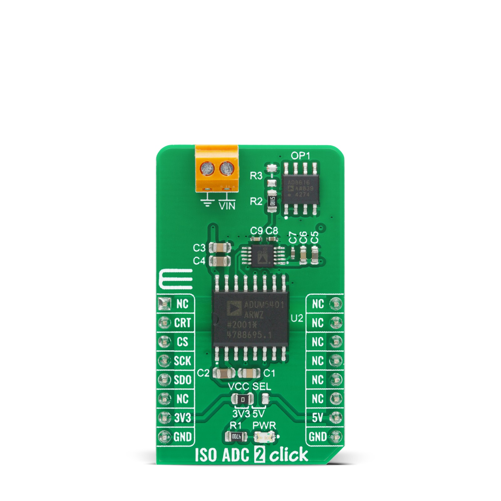
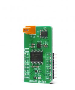
ISO ADC 2 Click is based on the AD7091R, a 12-bit successive-approximation analog-to-digital converter (ADC) with an isolated DC-DC converter, from Analog Devices. This Click board™ allows single-supply operation and consists of three Analog Devices active components: AD8616 a level shifting circuit, AD7091R an ADC stage and ADuM5401 an output isolation stage. The AD8616 is chosen for this application because of its low offset voltage, low bias current, and low noise. The output of the OpAmp is 0.1 V to 2.4 V which matches the input range of the ADC (0 V to 2.5 V) with a 100 mV safety margin to maintain linearity. A single-pole RC filter (R2/C9) follows the OpAmp output stage to reduce the out-of-band noise.
The next part of the circuit is the AD7091R, ADC that is chosen because of its ultralow power which is significantly lower than any competitive A/D converter. It features a power-down option, implemented across the serial interface to save power between conversions, described in the Modes of Operation section in the datasheet. After a successful conversion, the ADC sends the data to the MCU that goes through galvanic isolation provided by the ADuM5401 quad-channel digital isolator with an integrated DC-DC converter. The isolator has a secondary side controller architecture with isolated pulse-width modulation (PWM) feedback, and it works on the principle that is common to most switching power supplies.
The ISO ADC 2 Click communicates with MCU using the 3-wire SPI serial interface that operates at clock rates up to 50 MHz used for accessing data from the result register and controlling the modes of operation of the device. The CONVST signal of the AD7091R routed to the RST pin on the mikroBUS™ is used to initiate the conversion process, data acquisition, and to select the mode of operation. This ADC requires the user to initiate a software reset upon Power-Up, and it should be noted that failure to apply the correct software reset command may result in a device malfunction.
This Click Board™ uses the SPI communication interface with both 3.3V and 5V. The onboard SMD jumper labeled as VCC SEL allows voltage selection for interfacing with both 3.3V and 5V MCUs. More information about the AD7091R’s functionality, electrical specifications, and typical performance can be found in the attached datasheet. However, the Click board™ comes equipped with a library that contains easy to use functions and a usage example that may be used as a reference for the development.
Specifications
Type
ADC,Isolators
Applications
Can be used for a wide variety of industrial measurements, data acquisition systems, monitoring functions, and many more.
On-board modules
ISO ADC 2 Click is based on the AD7091R, a 12-bit successive-approximation analog-to-digital converter (ADC) with an isolated DC-DC converter, from Analog Devices.
Key Features
Low power consumption, fast throughput rate, wide input bandwidth, and more.
Interface
GPIO,SPI
Feature
No ClickID
Compatibility
mikroBUS™
Click board size
M (42.9 x 25.4 mm)
Input Voltage
3.3V or 5V
Pinout diagram
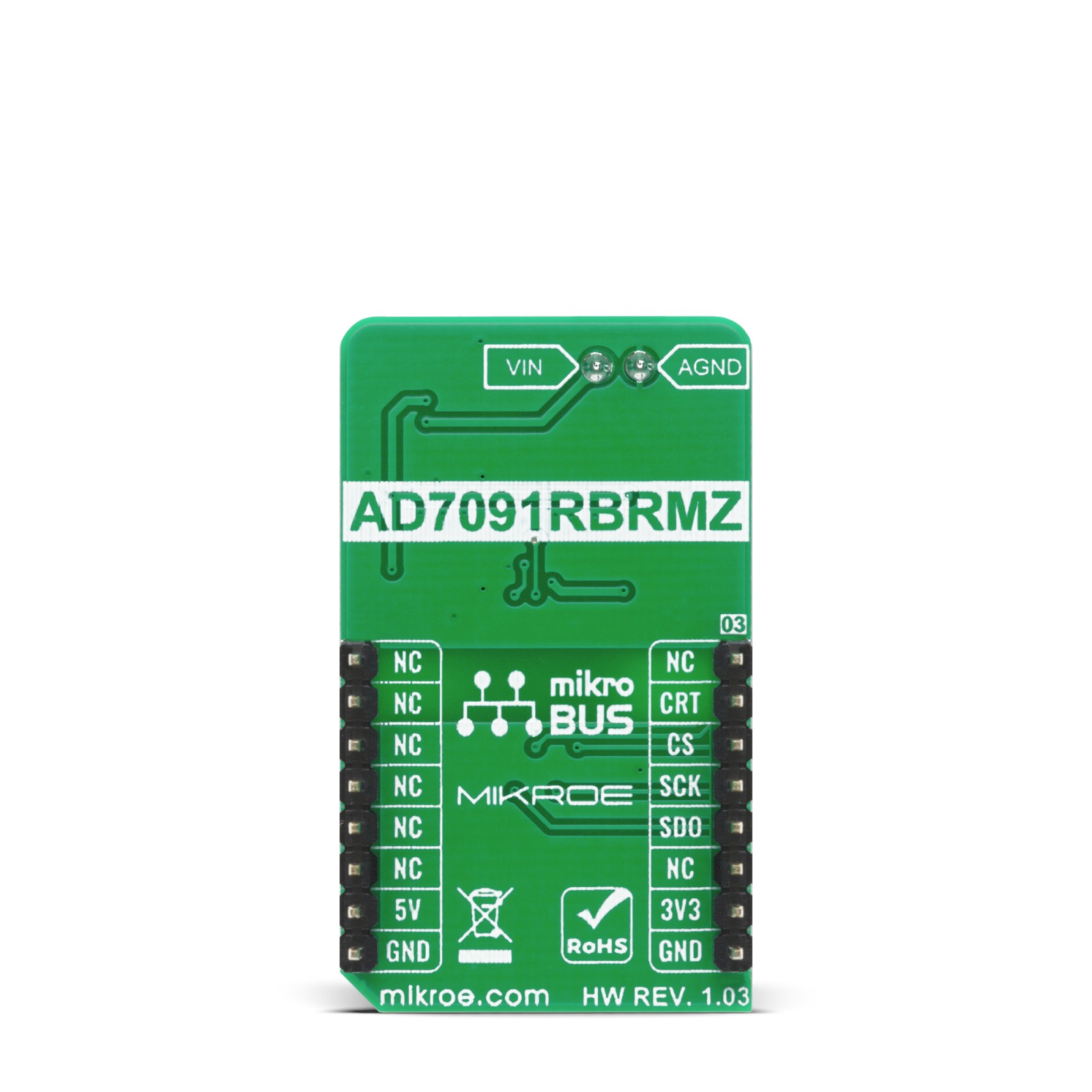
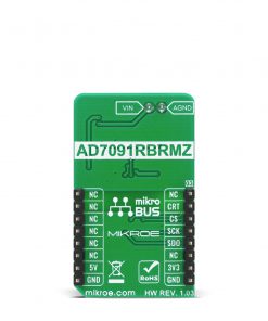
This table shows how the pinout on ISO ADC 2 Click corresponds to the pinout on the mikroBUS™ socket (the latter shown in the two middle columns).
Onboard settings and indicators
Label | Name | Default | Description |
---|---|---|---|
LD1 | PWR | – | Power LED Indicator |
JP1 | VCC SEL | Left | Power Supply Voltage Selection 3V3/5V: Left position 3V3, Right position 5V |
ISO ADC 2 Click electrical specifications
Description | Min | Typ | Max | Unit |
---|---|---|---|---|
Supply Voltage | 3.3 | – | 5 | V |
Analog Input VIN | 0 | – | 2.5 | V |
Resolution | 12 | – | – | bits |
Software Support
We provide a library for the ISO ADC 2 Click on our LibStock page, as well as a demo application (example), developed using MikroElektronika compilers. The demo can run on all the main MikroElektronika development boards.
Library Description
Key functions:
uint16_t isoadc2_read_adc ( void )
– Function for reading 12bit ADC datauint16_t isoadc2_get_mv ( uint16_t adc_data )
– Function for converting ADC to mV data
Examples description
The application is composed of three sections :
- System Initialization – Initialization of SPI module and additional pins
- Application Initialization – Maps GPIO and SPI for selected MIKROBUS
- Application Task – Every second reads ADC data, it to mV and logs result
void application_task ( ) { char demo_txt[ 30 ]; uint16_t rx_data; uint16_t mv_data; rx_data = isoadc2_read_adc( ); mv_data = isoadc2_get_mv( rx_data ); WordToStr( rx_data, demo_txt ); mikrobus_logWrite( " - ADC: ", _LOG_TEXT ); mikrobus_logWrite( demo_txt, _LOG_LINE ); WordToStr( mv_data, demo_txt ); mikrobus_logWrite( " - VIN: ", _LOG_TEXT ); mikrobus_logWrite( demo_txt, _LOG_TEXT ); mikrobus_logWrite( " mV", _LOG_LINE ); mikrobus_logWrite( "---------------", _LOG_LINE ); Delay_ms( 1000 ); }
The full application code, and ready to use projects can be found on our LibStock page.
Other mikroE Libraries used in the example:
- Conversion
- SPI
- UART
Additional notes and informations
Depending on the development board you are using, you may need USB UART click, USB UART 2 click or RS232 click to connect to your PC, for development systems with no UART to USB interface available on the board. The terminal available in all MikroElektronika compilers, or any other terminal application of your choice, can be used to read the message.
mikroSDK
This Click board™ is supported with mikroSDK – MikroElektronika Software Development Kit. To ensure proper operation of mikroSDK compliant Click board™ demo applications, mikroSDK should be downloaded from the LibStock and installed for the compiler you are using.
For more information about mikroSDK, visit the official page.