FRAM 3 Click
R205.00 ex. VAT
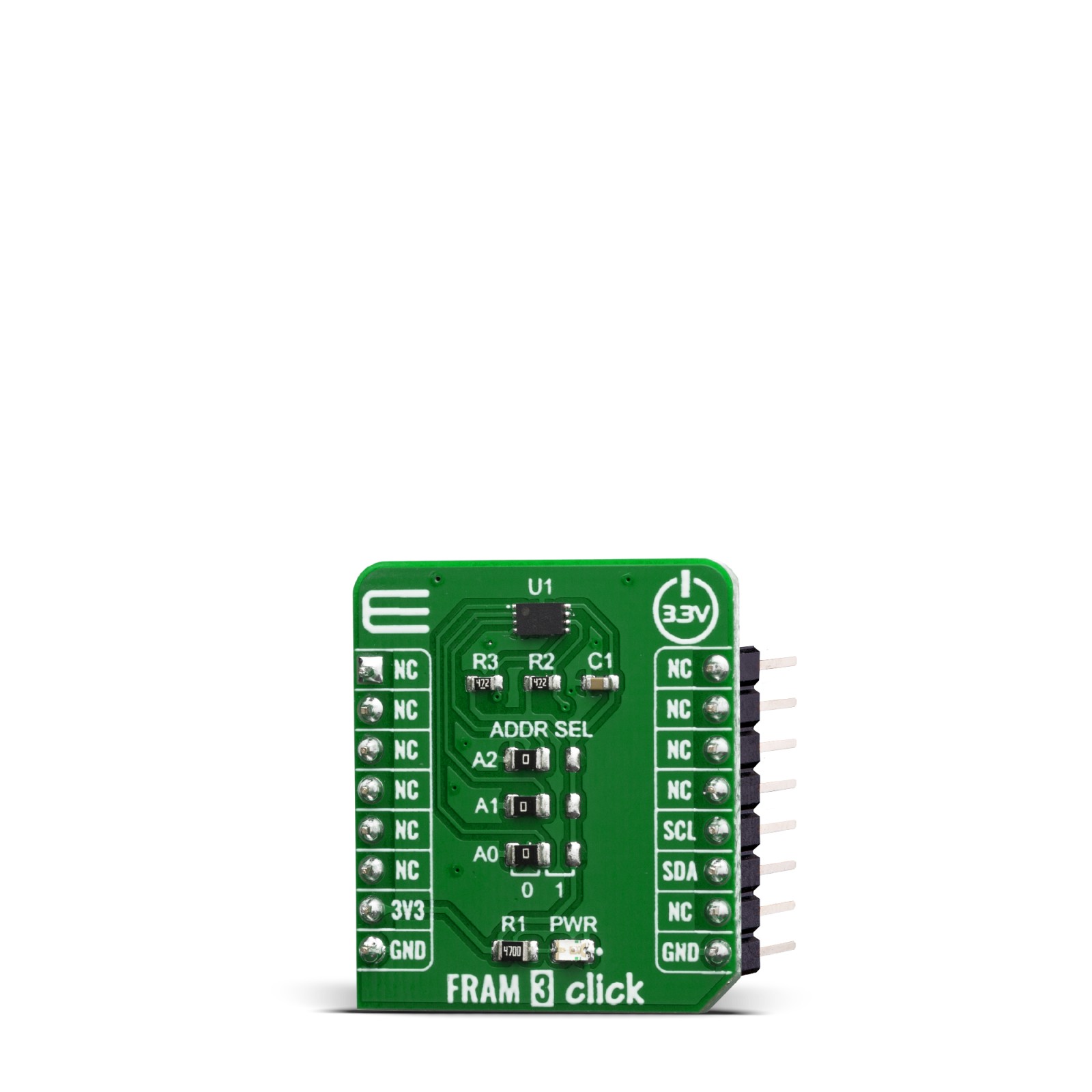
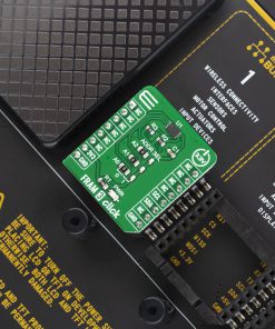
The FRAM 3 Click is a Click board™ that carries a ferroelectric RAM module. Ferroelectric RAM, also known as FRAM, is a non-volatile memory type, with characteristics that are comparable to much faster DRAM memory modules. It offers much faster alternative to common serial FLASH and EEPROM modules, which use the conventional technologies. FRAM 3 click uses the MB94R330, a serial FRAM module from Fujitsu Semiconductor LTD. FRAM embedded IC is proven utility in security applications such as IC cards.
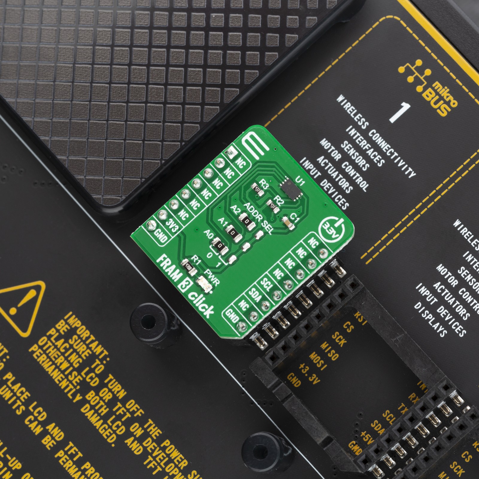
FRAM 3 click is supported by a mikroSDK compliant library, which includes functions that simplify software development. This Click board™ comes as a fully tested product, ready to be used on a system equipped with the mikroBUS™ socket.
Stock: Lead-time applicable.
| 5+ | R194.75 |
| 10+ | R184.50 |
| 15+ | R174.25 |
| 20+ | R167.69 |
How does it work?
The FRAM 3 click utilizes the MB94R330, which is an FRAM (Ferroelectric Random Access Memory) authentication IC using the ferroelectric process and silicon gate CMOS process technologies for forming the nonvolatile memory cells.
The MB94R330 adopts an original communication protocol based on the two-wire serial interface (I2C BUS), a hardware cryptographic macro and a proprietary control core. It is suitable for detecting cloned peripherals and accessories which is used in an electric equipment such as a printer, multifunction printer and so on.
.jpg)
Ferroelectric technology is still being developed and perfected, but the advantages have already been demonstrated. This technology exploits the properties of ferroelectric materials to retain the electric field after they have been exposed to it, the same way the ferromagnetic materials retain their magnetic field. This phenomenon is employed to polarize the FRAM cells and store the information. One of the areas that still need to be improved is the thermal instability, especially on high temperatures. When the ferroelectric material reaches the Curie temperature, its properties are degraded.
Therefore, the high temperature might damage the content of the FRAM module. This is illustrated by the data retention period: while working at 55˚C, the data retention period is 10 years. Still, combined with the endurance of 1010 read/write cycles at bus write speed, this type of memory still represents an ideal solution for applications that have to do a frequent writing to the non-volatile memory locations.
This Click board™ uses the I2C communication protocol, allowing very fast serial clock rates. To ensure reliable data transaction and to avoid accidental write to the memory array, the device employs certain protection mechanisms.
The MB94R330 supports the I2C bus, and operates as a slave device. The role of the communication for the I2C bus is different from “Master” side and “Slave” side. The master side has the authority to initiate control. Furthermore, the party line can be connected which connects two or more slave devices to one master. In this case, the slave side has each unique address respectively, and after specifying the address on the slave side, the master side starts to communicate.
The FRAM 3 click is suitable for detecting cloned peripherals and accessories which is used in an electric equipment such as a printer, multifunction printer and so on.
Specifications
Type
FRAM
Applications
It is suitable for detecting cloned peripherals and accessories which is used in an electric equipment such as a printer, multifunction printer and so on.
On-board modules
MB94R330, a serial FRAM module from Fujitsu Semiconductor LTD.
Key Features
Free access area 112 bytes, Resource counter area 4 bytes x 8 slot, ID area 8bytes x 4 slot
Interface
I2C
Feature
No ClickID
Compatibility
mikroBUS™
Click board size
S (28.6 x 25.4 mm)
Input Voltage
3.3V
Pinout diagram
This table shows how the pinout on FRAM 3 click corresponds to the pinout on the mikroBUS™ socket (the latter shown in the two middle columns).
Onboard settings and indicators
| Label | Name | Default | Description |
|---|---|---|---|
| JP1 | A0 | Left | Select address 0 |
| JP2 | A1 | Left | Select address 1 |
| JP3 | A2 | Left | Select address 2 |
Software Support
We provide a library for the FRAM 3 click on our LibStock page, as well as a demo application (example), developed using MikroElektronika compilers. The demo can run on all the main MikroElektronika development boards.
Library Description
Library provides control over reading and writing data via I2C module. You can use 2 specific functions for reading and writing to memory.
Key functions:
void fram3_read_data ( uint8_t *data_buf, uint8_t n_buf_size )– Generic read data functionvoid fram3_write_data ( uint8_t *data_buf, uint8_t n_buf_size )– Generic write data functionuint8_t fram3_read_free_access_memory ( uint8_t start_addr, uint8_t *data_buf, uint8_t n_buf_size )– Memory read functionuint8_t fram3_write_free_access_memory ( uint8_t start_addr, uint8_t *data_buf, uint8_t n_buf_size )– Memory write function
Examples description
The application is composed of three sections :
- System Initialization – Initializes I2C module
- Application Initialization – Initializes driver init
- Application Task – Writes and then reads data from memory
void application_task (  )
{
    mikrobus_logWrite( " - Writing... ", _LOG_LINE );
    Delay_ms( 500 );
    status_check = fram3_write_free_access_memory( 0x00, &write_data[ 0 ], 7 );
    if ( status_check == FRAM3_ERROR )
    {
        mikrobus_logWrite( " - ERROR WRITING!!! ", _LOG_LINE );
        for ( ; ; );
    }

    mikrobus_logWrite( " - Reading... ", _LOG_LINE );
    Delay_ms( 500 );
    status_check = fram3_read_free_access_memory( 0x00, &read_data[ 0 ], 7 );
    if ( status_check == FRAM3_ERROR )
    {
        mikrobus_logWrite( " - ERROR READING!!! ", _LOG_LINE );
        for ( ; ; );
    }

    for ( cnt = 0; cnt < 7; cnt++ )
    {
        mikrobus_logWrite( &read_data[ cnt ], _LOG_BYTE );
        Delay_ms( 100 );
    }
    mikrobus_logWrite( "", _LOG_LINE );
    Delay_ms( 1000 );
    mikrobus_logWrite( "__________________________", _LOG_LINE );
    Delay_ms( 500 );
}
The full application code, and ready to use projects can be found on our LibStock page.
Other mikroE Libraries used in the example:
- I2C
- UART
Additional notes and informations
Depending on the development board you are using, you may need USB UART click, USB UART 2 click or RS232 click to connect to your PC, for development systems with no UART to USB interface available on the board. The terminal available in all MikroElektronika compilers, or any other terminal application of your choice, can be used to read the message.
mikroSDK
This Click board™ is supported with mikroSDK – MikroElektronika Software Development Kit. To ensure proper operation of mikroSDK compliant Click board™ demo applications, mikroSDK should be downloaded from the LibStock and installed for the compiler you are using.
For more information about mikroSDK, visit the official page.
Resources
Downloads
| Weight | 25 g |
|---|---|
| Brand | MikroElektronika |


