How does it work?
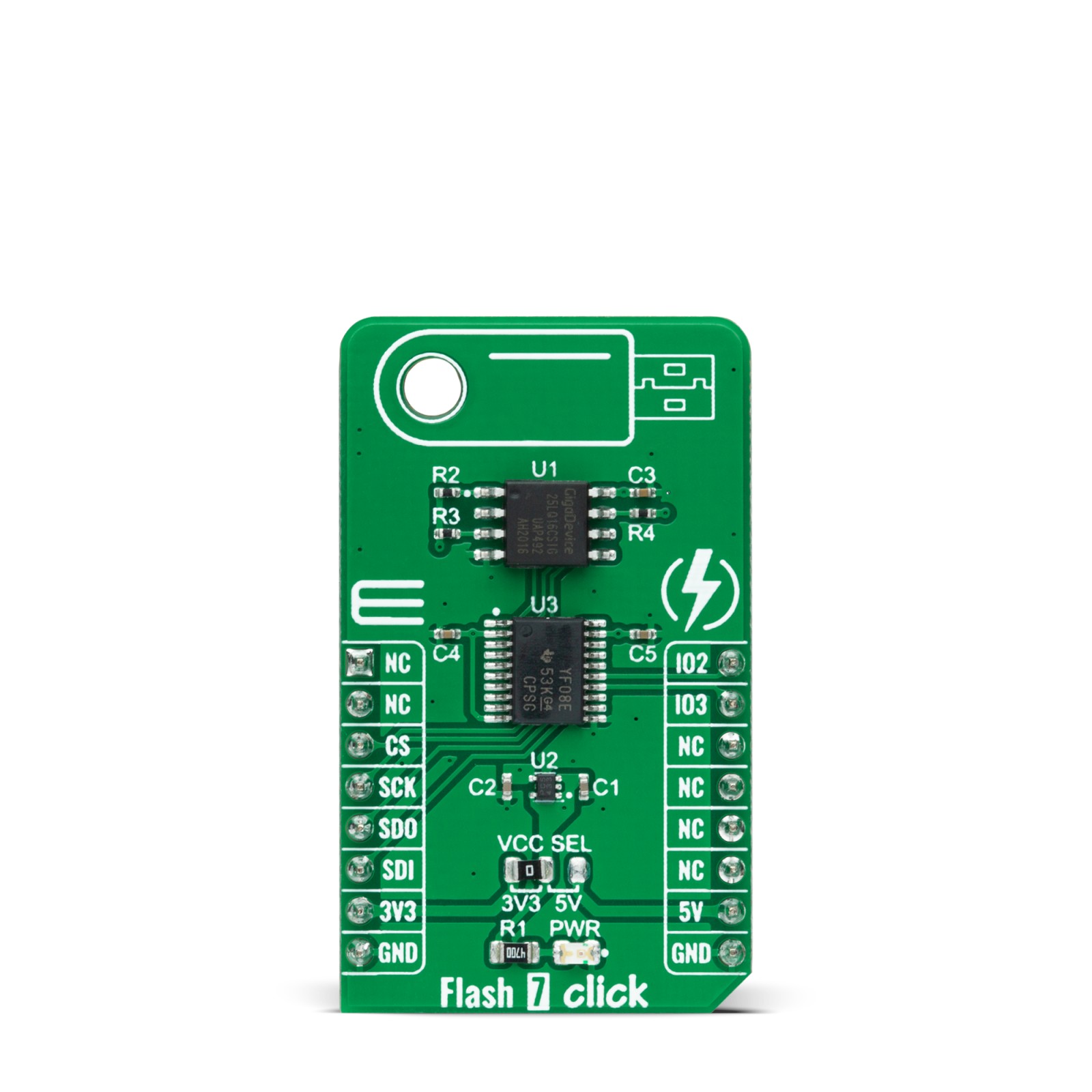
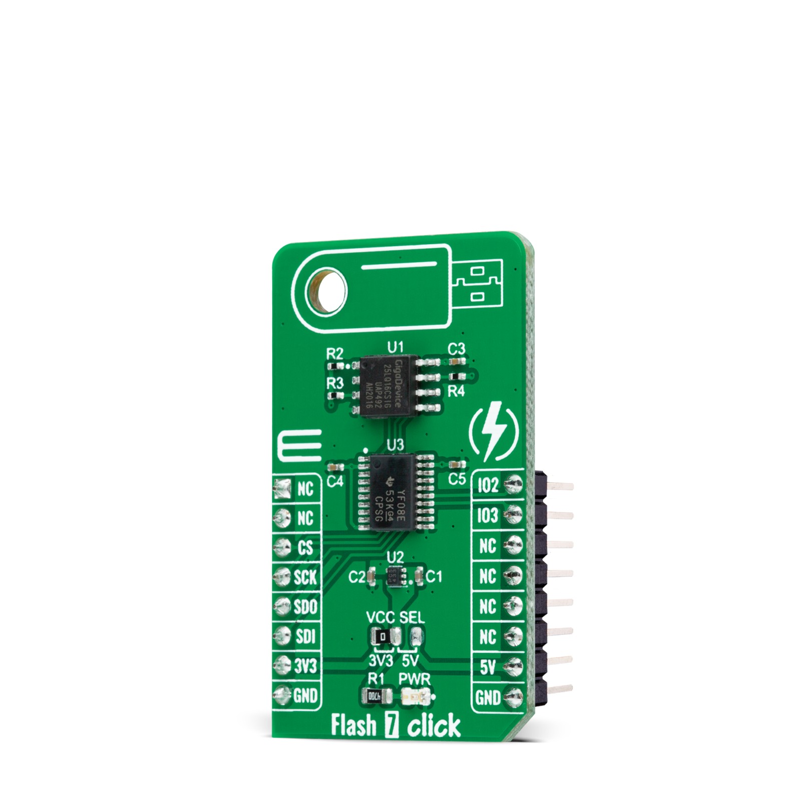
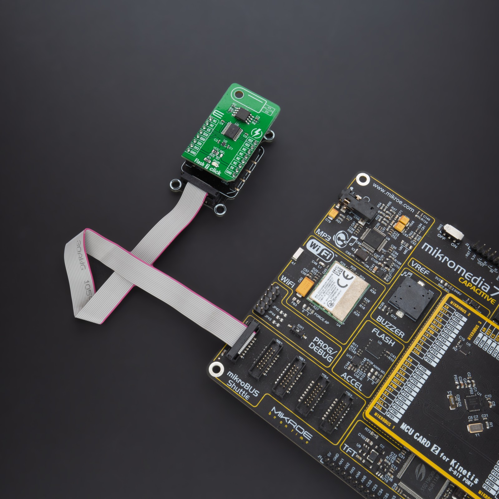
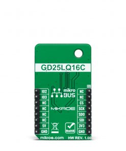
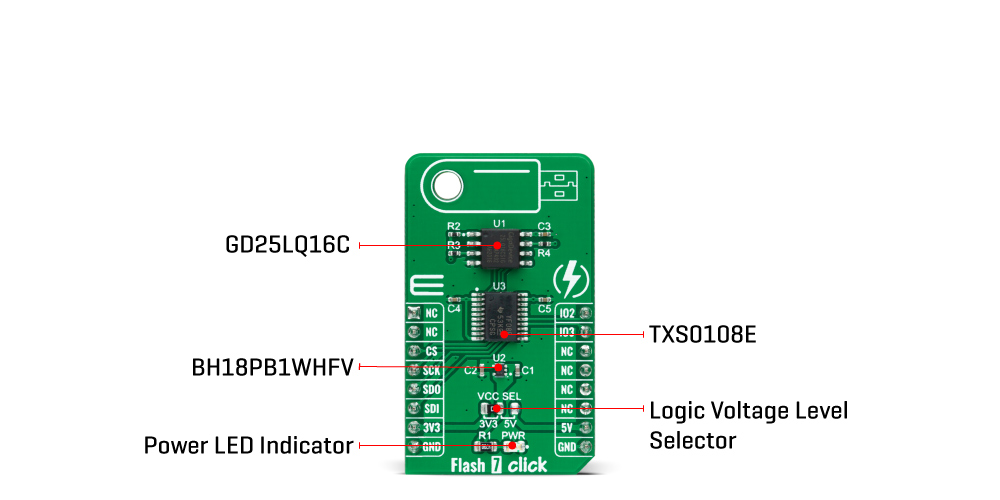
Flash 7 Click is based on the GD25LQ16C, a high-performance 16Mbit SPI NOR Flash Memory solution with advanced security features from GigaDevice Semiconductor. Requiring only 6 signals to communicate between the MCU and the memory thus reduces the design complexity and offers a reduction in board space and total system cost. It is specifically designed to meet the different needs in various electronic applications in terms of density, performance, reliability, and security while providing low power consumption.
This Click board™ includes an LDO regulator BH18PB1WHFV from Rohm Semiconductor to provide the 1.8 V supply voltage. The LDO cut power consumption by lowering its current consumption to approximately 2 μA when the application is operating in the standby state. The output from the LDO regulator is providing a needed reference voltage for one side of the TXS0108E, an 8-bit bidirectional level shifting and voltage translator for open-drain and push-pull applications from Texas Instruments. The reference voltage for the other side of the level shifter is taken from the 3.3V pin from the mikroBUS™.
Flash 7 Click communicates with MCU using the SPI serial interface that supports the Dual/Quad SPI and the two most common modes, SPI Mode 0 and 3, with a maximum SPI frequency of 104 MHz. The Dual I/O data is transferred with a speed of 208 Mbits/s, and the Quad I/O data with a speed of 416 Mbits/s. In addition to the SPI communication, the Flash 7 Click also has two additional pins used for Write Protection and HOLD function routed to the PWM and INT pins of the mikroBUS™ socket.
The HOLD pin, labeled as IO3, can be used to pause the serial communication with the device without having to stop the operation of write status register, programming, or erasing in progress. On the other side, the configurable Write Protection function labeled as IO2 serves to protect the memory array contents via the Software Protection Mode.
This Click board™ is designed to operate with both 3.3V and 5V logic voltage levels selected via the VCC SEL jumper. It allows for both 3.3V and 5V capable MCUs to use the SPI communication lines properly. However, the Click board™ comes equipped with a library that contains easy to use functions and an example code which can be used, as a reference, for further development.
Specifications
Type
FLASH
Applications
Can be used to provides a storage solution for systems with limited space in various embedded applications.
On-board modules
Flash 7 Click is based on the GD25LQ16C, a high-performance SPI NOR Flash Memory solution with advanced security features from GigaDevice Semiconductor.
Key Features
Low power consumption, high performance, reliability, advanced security features, data retention, and more.
Interface
QSPI,SPI
Feature
No ClickID
Compatibility
mikroBUS™
Click board size
M (42.9 x 25.4 mm)
Input Voltage
3.3V or 5V
Pinout diagram
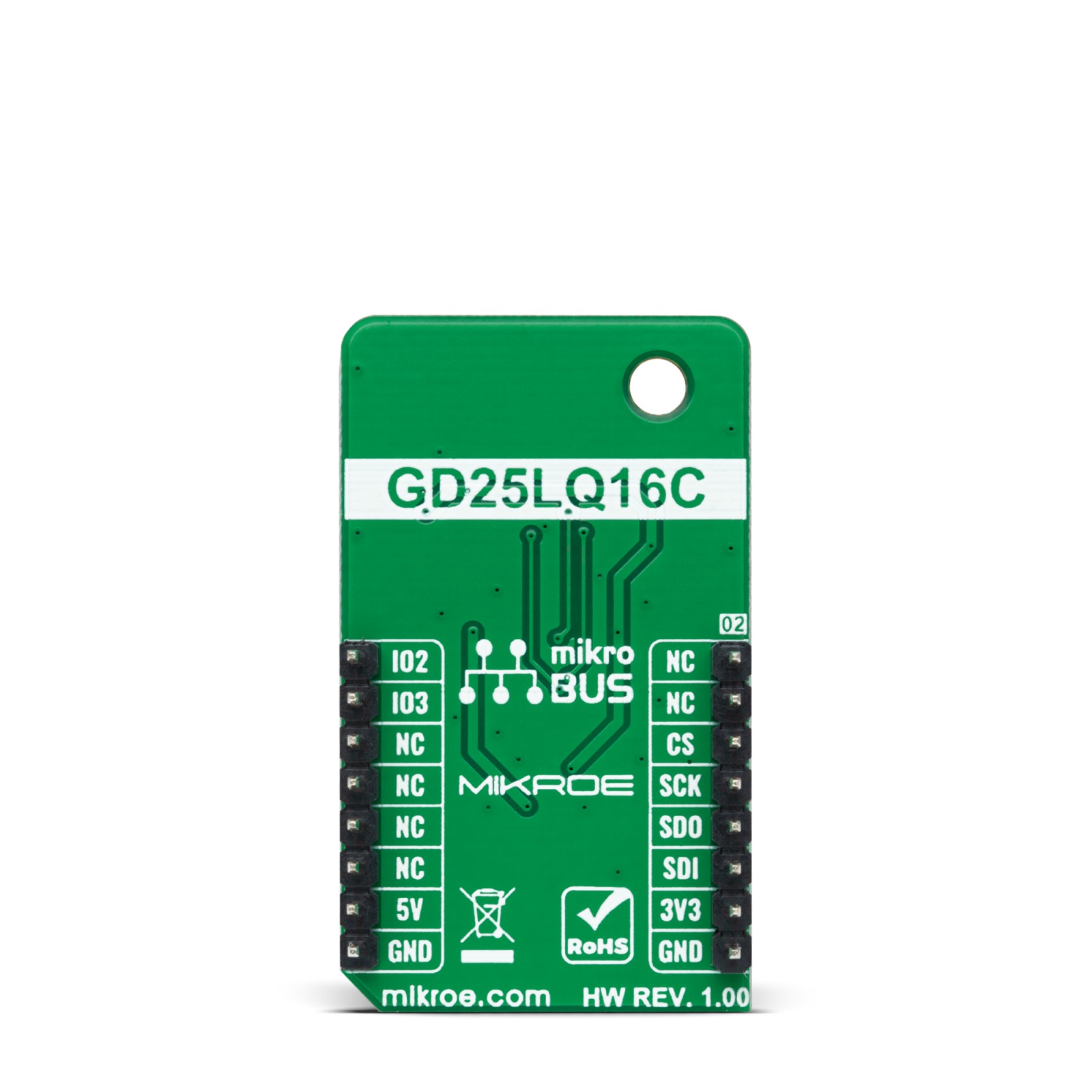
This table shows how the pinout on Flash 7 Click corresponds to the pinout on the mikroBUS™ socket (the latter shown in the two middle columns).
Onboard settings and indicators
Label | Name | Default | Description |
---|---|---|---|
LD1 | PWR | – | Power LED Indicator |
JP1 | VCC SEL | Left | Power Supply Voltage Selection 3V3/5V: Left position 3V3, Right position 5V |
Flash 7 Click electrical specifications
Description | Min | Typ | Max | Unit |
---|---|---|---|---|
Supply Voltage | 2.5 | – | 5.5 | V |
Memory Size | – | – | 16 | Mbit |
Data Retention | – | 20 | – | Years |
Clock Frequency | – | – | 104 | MHz |
Operating Temperature Range | -40 | – | +85 | °C |
Software Support
We provide a library for the Flash 7 Click on our LibStock page, as well as a demo application (example), developed using MikroElektronika compilers. The demo can run on all the main MikroElektronika development boards.
Library Description
The library covers all the necessary functions to control Flash 7 Click board™. Library performs a standard SPI interface communication.
Key functions:
void flash7_chip_erase ( void )
– Chip erase function.uint8_t flash7_page_program ( uint32_t mem_addr, uint8_t *p_tx_data, uint16_t n_bytes )
– Page program function.void flash7_read_memory ( uint32_t mem_addr, uint8_t *p_rx_data, uint16_t n_bytes )
– Read memory function.
Examples description
The application is composed of three sections :
- System Initialization – Initializes SPI and UART LOG, sets CS, PWM and INT pins as outputs.
- Application Initialization – Initialization driver enables SPI, disables write protect and hold, performs whole chip erase, targets the memory address at “4096” for page program starting point and writes data which is also displayed on the log.
- Application Task – This is an example that demonstrates the use of the Flash 7 Click board™. In this example, the data is read from the targeted memory address. The results are being sent to the Usart Terminal. This task repeats every 5 sec.
void application_task ( ) { mikrobus_logWrite( "-----------------------", _LOG_LINE ); mikrobus_logWrite( "<- Read data : ", _LOG_TEXT ); flash7_read_memory( memory_addr, &rx_data[ 0 ], 9 ); mikrobus_logWrite( rx_data, _LOG_LINE ); Delay_ms( 5000 ); }
The full application code, and ready to use projects can be found on our LibStock page.
Other mikroE Libraries used in the example:
- SPI
- UART
Additional notes and informations
Depending on the development board you are using, you may need USB UART click, USB UART 2 click or RS232 click to connect to your PC, for development systems with no UART to USB interface available on the board. The terminal available in all MikroElektronika compilers, or any other terminal application of your choice, can be used to read the message.
mikroSDK
This Click board™ is supported with mikroSDK – MikroElektronika Software Development Kit. To ensure proper operation of mikroSDK compliant Click board™ demo applications, mikroSDK should be downloaded from the LibStock and installed for the compiler you are using.
For more information about mikroSDK, visit the official page.