Flash 13 Click
R170.00 ex. VAT
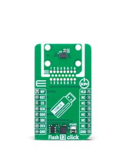
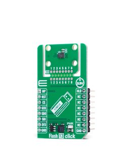
Flash 13 Click is a compact add-on board designed for fast and reliable data storage in embedded applications. This board features the BY25Q16E, a 16Mbit SPI NOR Flash memory chip from BYTe Semiconductor. It supports standard, Dual, and Quad SPI interfaces with clock speeds up to 108MHz, enabling high-speed data transfer rates up to 432MHz in Quad mode. It features Continuous Read Mode for true XIP (execute-in-place) operation, three 1024-byte security registers for secure data storage, and endurance of 100,000 program/erase cycles per sector with 20-year data retention. Communication is handled via SPI using 3.3V logic and introduces the innovative Click Snap feature for flexible chip placement with additional HOLD and Write Protect functions for advanced control. Flash 13 Click is ideal for use in both commercial and industrial environments that require high-performance, secure, and long-lasting non-volatile memory.
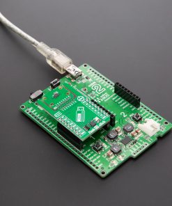
Flash 13 Click is fully compatible with the mikroBUS™ socket and can be used on any host system supporting the mikroBUS™ standard. It comes with the mikroSDK open-source libraries, offering unparalleled flexibility for evaluation and customization. What sets this Click board™ apart is the groundbreaking ClickID feature, enabling your host system to seamlessly and automatically detect and identify this add-on board, alongside a Click Snap feature introducing a new level of flexibility and ease of use.
Stock: Lead-time applicable.
| 5+ | R161.50 |
| 10+ | R153.00 |
| 15+ | R144.50 |
| 20+ | R139.06 |
How does it work?
Flash 13 Click is based on the BY25Q16E, a 16Mbit SPI NOR Flash memory from BYTe Semiconductor. This memory supports a range of communication modes including standard SPI, Dual/Quad I/O SPI, and a 2-clock instruction cycle Quad Peripheral Interface (QPI), offering flexibility for embedded applications. With SPI clock frequencies reaching up to 108MHz, the BY25Q16E can achieve data transfer rates of up to 216MHz in Dual I/O mode and an impressive 432MHz in Quad I/O mode when utilizing Fast Read or QPI instructions. These high-speed operations enable performance levels that surpass those of traditional asynchronous 8-bit and 16-bit parallel flash memories, making it suitable for demanding commercial and industrial use cases that demand fast access, secure storage, and extended operational lifetime. The BY25Q16E offers high endurance with a typical lifespan of 100,000 program-erase cycles per sector and long-term reliability with a typical data retention period of 20 years.

One of the standout features of the BY25Q16E is its Continuous Read Mode, which enables quick memory access by requiring just 8 clock cycles to read a 24-bit address. This capability makes true XIP (execute in place) operations possible, significantly optimizing system performance where direct code execution from Flash is required. The device also adheres to JEDEC standards by supporting standard manufacturer and device ID protocols, and it incorporates three security registers of 1024 bytes each for data protection and secure storage requirements.
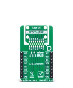
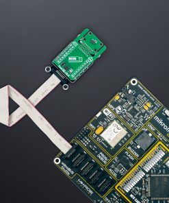
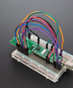
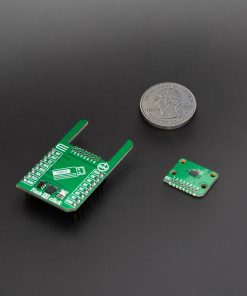
This Click board™ is designed in a unique format supporting the newly introduced MIKROE feature called “Click Snap.” Unlike the standardized version of Click boards, this feature allows the main chip area to become movable by breaking the PCB, opening up many new possibilities for implementation. Thanks to the Snap feature, the BY25Q16E can operate autonomously by accessing their signals directly on the pins marked 1-8. Additionally, the Snap part includes a specified and fixed screw hole position, enabling users to secure the Snap board in their desired location.
Flash 13 Click communicates with MCU through a standard SPI interface supporting the two most common SPI modes, SPI Mode 0 and 3, and a maximum clock frequency of up to 108MHz. The BY25Q16E enhances data transfer rates through Dual and Quad SPI operations, which double and quadruple the standard SPI speed, respectively. These enhanced speeds are achieved by re-purposing the available pins as bidirectional I/O pins during Dual and Quad SPI operations.
Furthermore, the board features a HOLD function, marked as HLD and routed on the default position of the PWM pin of the mikroBUS™ socket. The hold function allows the suspension of serial communications without disrupting ongoing operations. The board also has a Write Protect feature, marked as WP and routed on the default position of the AN of the mikroBUS™ socket, that safeguards all registers and memory from unintended write operations through both hardware and software mechanisms.
This Click board™ can be operated only with a 3.3V logic voltage level. The board must perform appropriate logic voltage level conversion before using MCUs with different logic levels. It also comes equipped with a library containing functions and example code that can be used as a reference for further development.
Click Snap
Click Snap is an innovative feature of our standardized Click add-on boards, introducing a new level of flexibility and ease of use. This feature allows for easy detachment of the main sensor area by simply snapping the PCB along designated lines, enabling various implementation possibilities. For detailed information about Click Snap, please visit the official page dedicated to this feature.
Specifications
Type
FLASH
Applications
Ideal for use in both commercial and industrial environments that require high-performance, secure, and long-lasting non-volatile memory
On-board modules
BY25Q16E – 16Mb SPI NOR flash from BYTe Semiconductor
Key Features
SPI NOR Flash memory, 16Mbit capacity, standard SPI, Dual I/O SPI, Quad I/O SPI, QPI interface, Continuous Read Mode, XIP (execute in place) support, JEDEC-compliant ID, three 1024-byte security registers, 100,000 program/erase cycles endurance, 20-year data retention, and more
Interface
QSPI,SPI
Feature
Click Snap,ClickID
Compatibility
mikroBUS™
Click board size
M (42.9 x 25.4 mm)
Input Voltage
3.3V
Pinout diagram
This table shows how the pinout on Flash 13 Click corresponds to the pinout on the mikroBUS™ socket (the latter shown in the two middle columns).
| Notes | Pin | Pin | Notes | ||||
|---|---|---|---|---|---|---|---|
| Write Protect / IO2 | WP | 1 | AN | PWM | 16 | HLD | Communication Pause / IO3 |
| ID SEL | RST | 2 | RST | INT | 15 | NC | |
| SPI Select / ID COMM | CS | 3 | CS | RX | 14 | NC | |
| SPI Clock | SCK | 4 | SCK | TX | 13 | NC | |
| SPI Data OUT / IO1 | SDO | 5 | MISO | SCL | 12 | NC | |
| SPI Data IN / IO0 | SDI | 6 | MOSI | SDA | 11 | NC | |
| Power Supply | 3.3V | 7 | 3.3V | 5V | 10 | NC | |
| Ground | GND | 8 | GND | GND | 9 | GND | Ground |
Onboard settings and indicators
| Label | Name | Default | Description |
|---|---|---|---|
| LD1 | PWR | – | Power LED Indicator |
Flash 13 Click electrical specifications
| Description | Min | Typ | Max | Unit |
|---|---|---|---|---|
| Supply Voltage | – | 3.3 | – | V |
| Memory Size | – | – | 16 | Mbit |
| Write Endurance | 100k | – | – | Cycles |
| Data Retention | 20 | – | – | Years |
Software Support
Flash 13 Click demo application is developed using the NECTO Studio, ensuring compatibility with mikroSDK‘s open-source libraries and tools. Designed for plug-and-play implementation and testing, the demo is fully compatible with all development, starter, and mikromedia boards featuring a mikroBUS™ socket.
Example Description
This example demonstrates the use of Flash 13 Click board by writing specified data to the memory and reading it back.
Key Functions
flash13_cfg_setupThis function initializes Click configuration structure to initial values.flash13_initThis function initializes all necessary pins and peripherals used for this Click board.flash13_erase_memoryThis function erases the selected amount of memory which contains the selected address.flash13_memory_writeThis function writes a desired number of data bytes starting from the selected memory address.flash13_memory_readThis function reads a desired number of data bytes starting from the selected memory address.
Application Init
Initializes the driver and checks the communication by reading and verifying the device ID.
Application Task
Writes a desired number of bytes to the memory and then verifies if it is written correctly by reading from the same memory location and displaying the memory content on the USB UART. The whole 4KB sector of memory that contains the STARTING_ADDRESS will be erased before writing data.
Application Output
This Click board can be interfaced and monitored in two ways:
- Application Output – Use the “Application Output” window in Debug mode for real-time data monitoring. Set it up properly by following this tutorial.
- UART Terminal – Monitor data via the UART Terminal using a USB to UART converter. For detailed instructions, check out this tutorial.
Additional Notes and Information
The complete application code and a ready-to-use project are available through the NECTO Studio Package Manager for direct installation in the NECTO Studio. The application code can also be found on the MIKROE GitHub account.
Resources
Downloads
| Weight | 17 g |
|---|---|
| Brand | MikroElektronika |