How does it work?
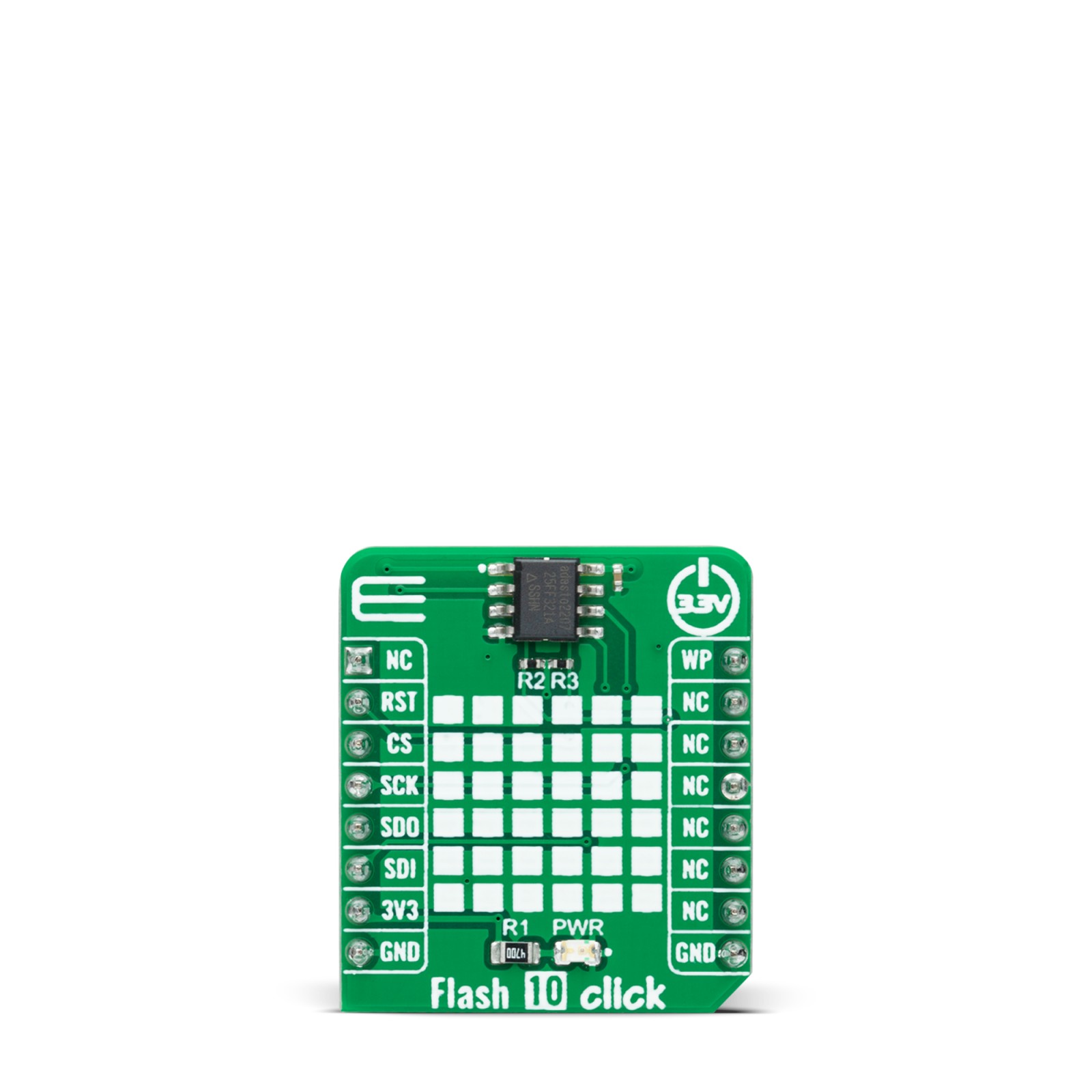
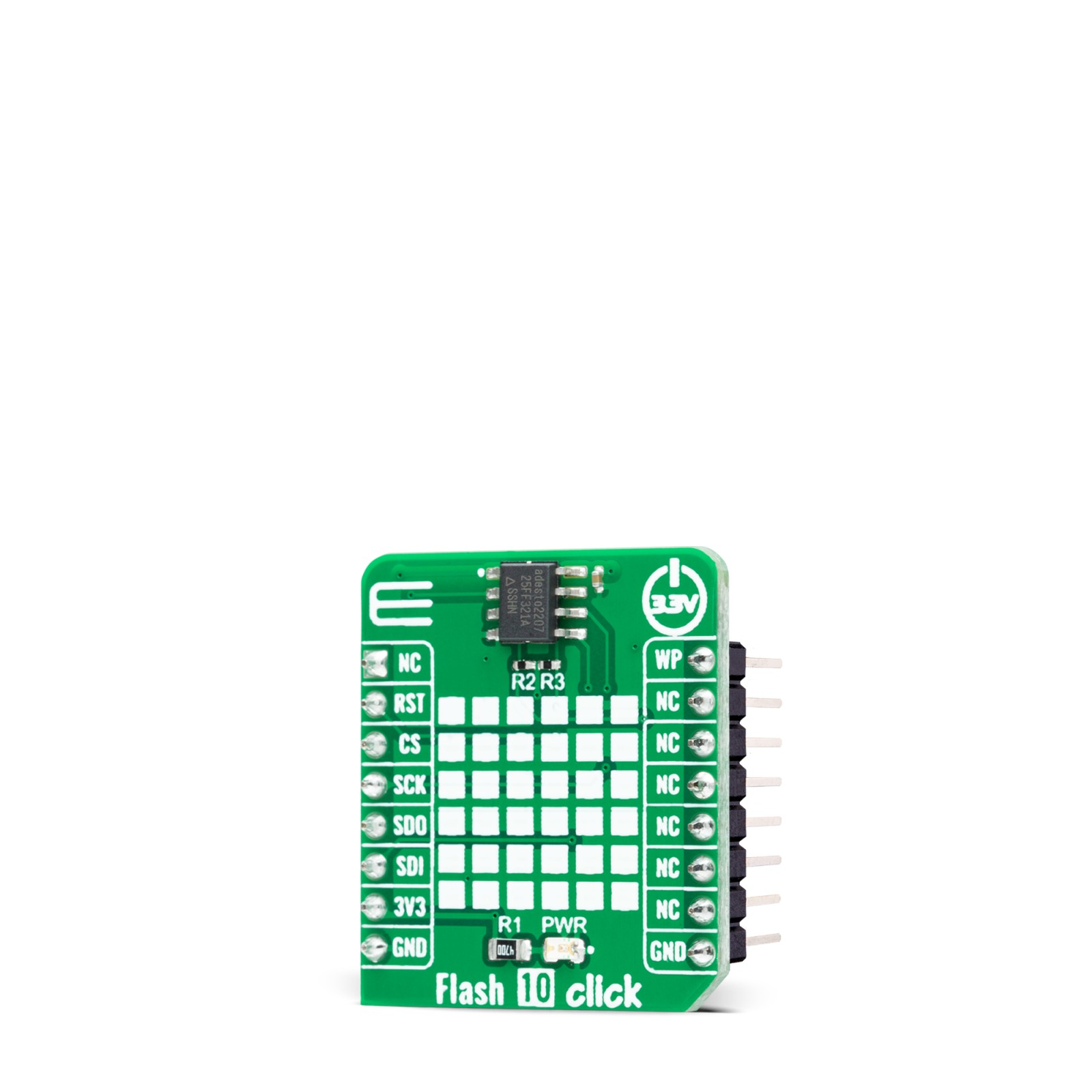
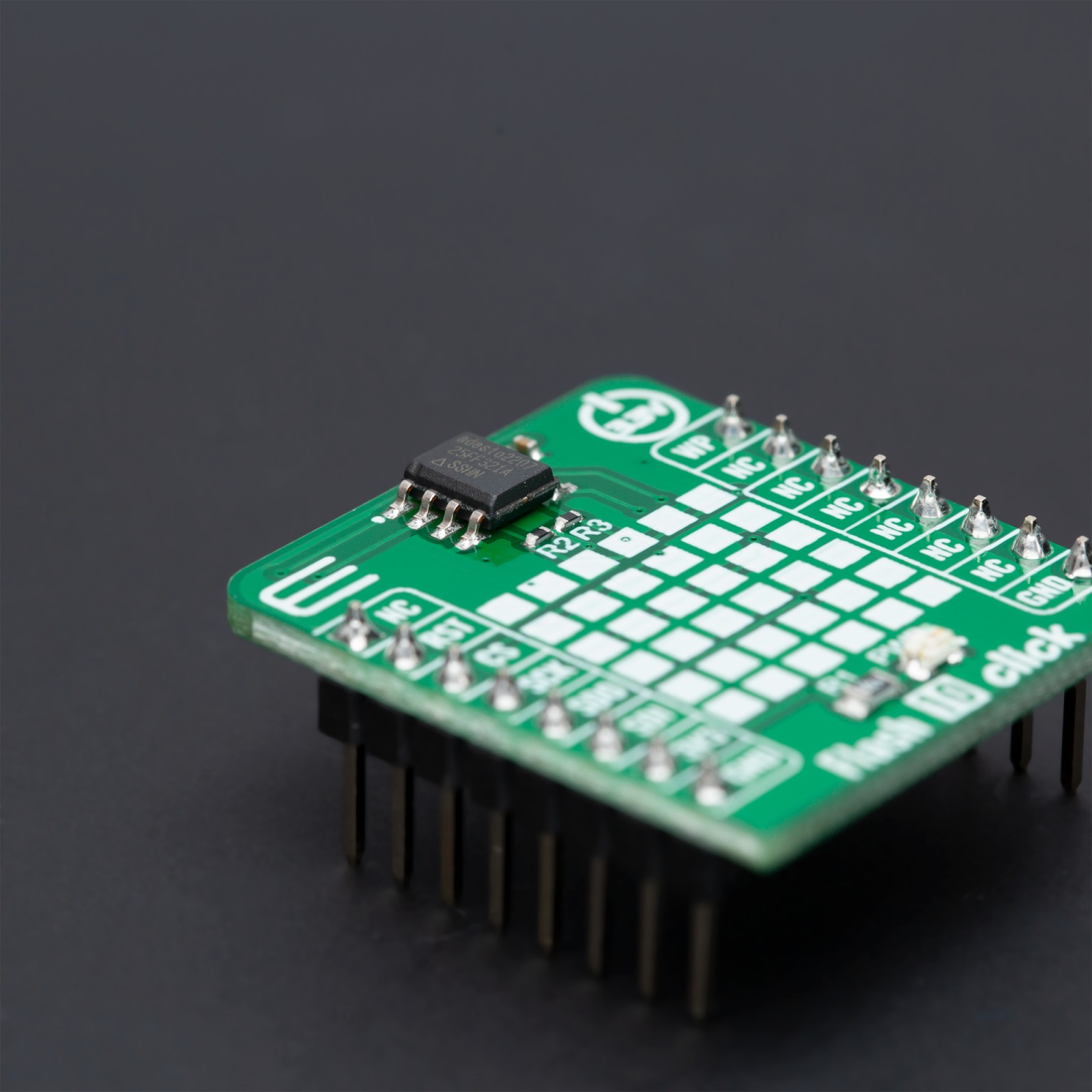
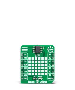
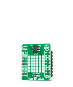
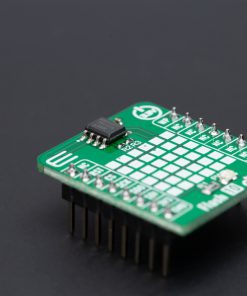
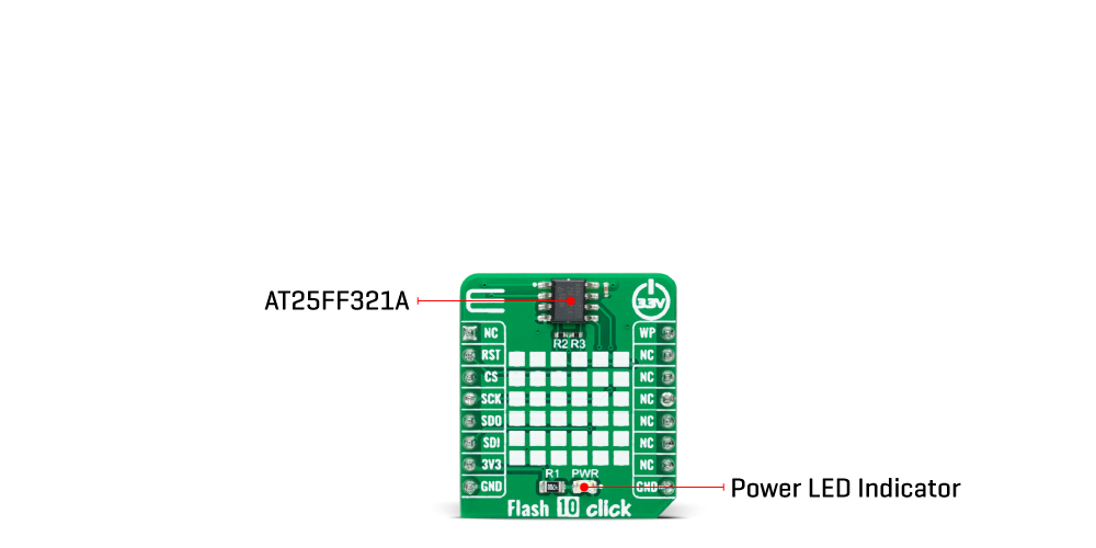
Flash 10 Click as its foundation uses the AT25FF321A, a highly reliable serial Flash memory solution designed for use in a wide variety of high-volume consumer and connected applications from Dialog Semiconductor. The AT25FF321A is organized as a 32Mbit (16×2 Mbit physical block) Flash memory ideally suited for systems in which program code is shadowed from Flash memory into embedded or external RAM (code shadow) for execution and where small amounts of data are stored and updated locally in the Flash memory. The AT25FF321A specifies a minimum of 100.000 endurance cycles with data retention of a minimum of 20 years, giving it the capability to handle unlimited reads/writes to the memory.
The AT25FF321A’s erase block sizes are optimized to meet the needs of today’s code and data storage applications, supporting flexible and optimized erase architecture for code and data storage applications (4kB, 32kB, and 64kB block erase operations) and a full-chip erase feature. The most efficient use of memory space can be achieved by optimizing the erase blocks’ size. Also, the AT25FF321A contains four specialized 128-byte One-Time Programmable (OTP) security registers which can be used to store a unique device ID and locked key storage.
Flash 10 Click communicates with MCU through a standard SPI interface supporting the two most common SPI modes, SPI Mode 0 and 3. Furthermore, this Click board™ provides additional hardware-controlled functions. The configurable Write Protection, marked as WP and routed on the PWM pin of the mikroBUS™ socket, protects all registers (including status and configuration) from write operations and must be held low to inhibit all the write operations to registers. When this pin is low, all memory and register writes are prohibited, and the address counter is not incremented.
Also, it is possible to use the Reset or Hold function through the RST pin of the mikroBUS™ socket, depending on the state of the HOLD/RESET bit 7 in Status Register 3. In the case of the Hold function, this pin temporarily pauses serial communication without deselecting or resetting the device, while in the case of the Reset feature, a low logic level on the RST pin puts the AT25FF321A into a Reset state.
This Click board™ can be operated only with a 3.3V logic voltage level. The board must perform appropriate logic voltage level conversion before using MCUs with different logic levels. However, the Click board™ comes equipped with a library containing functions and an example code that can be used, as a reference, for further development.
Specifications
Type
FLASH
Applications
Can be used for storage and data transfer in consumer devices, enterprise systems, and industrial applications
On-board modules
AT25FF321A – serial Flash memory solution from Dialog Semiconductor
Key Features
32Mbit (16x2Mbit physical block) flash memory, optimized erase architecture for code and data storage applications, flexible non-volatile block protection, high performance, write protection, data endurance and retention, low power consumption, and more
Interface
QSPI,SPI
Feature
No ClickID
Compatibility
mikroBUS™
Click board size
S (28.6 x 25.4 mm)
Input Voltage
3.3V
Pinout diagram
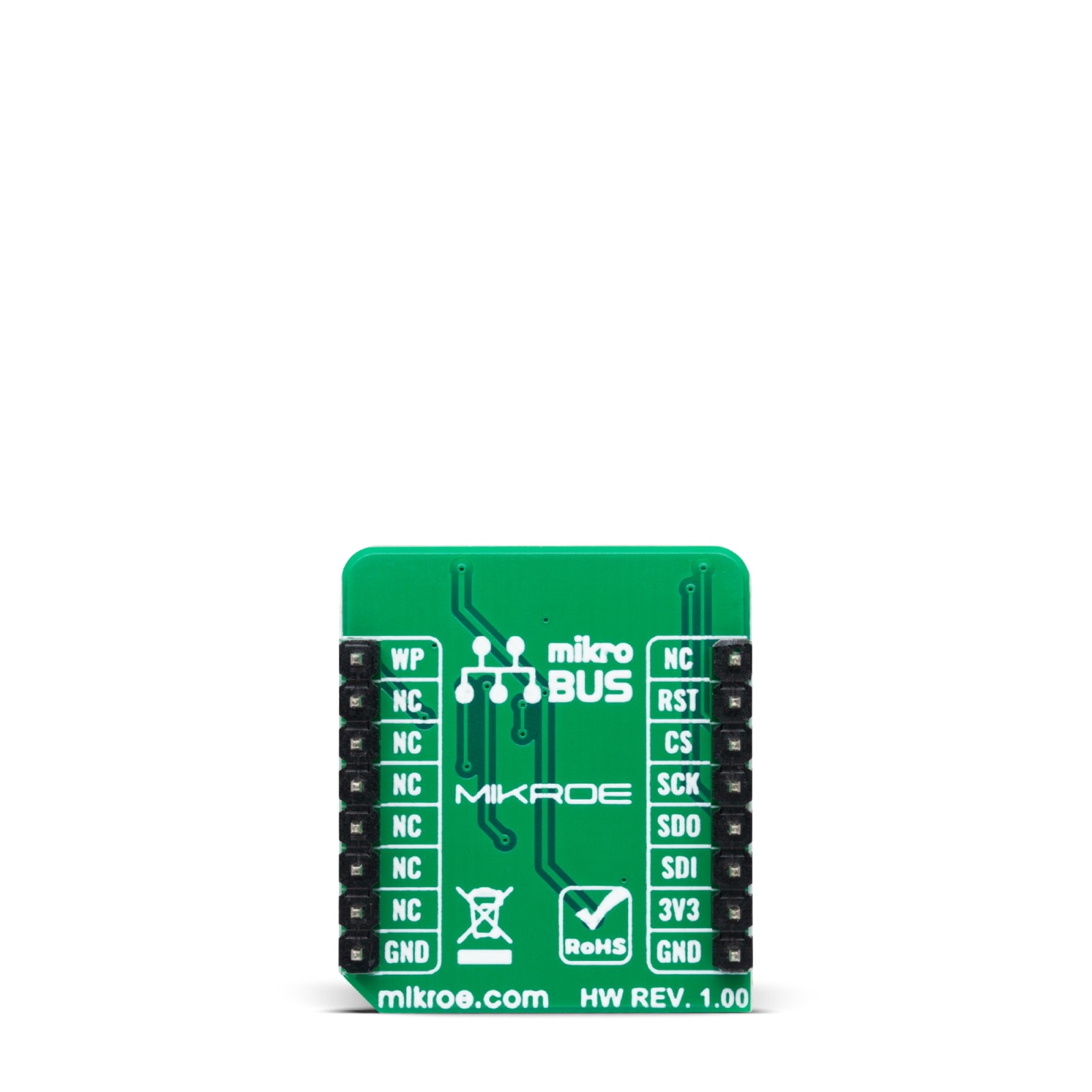
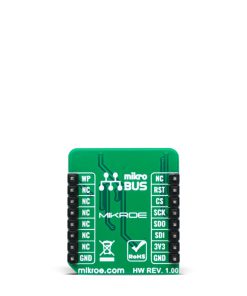
This table shows how the pinout on Flash 10 Click corresponds to the pinout on the mikroBUS™ socket (the latter shown in the two middle columns).
Onboard settings and indicators
Label | Name | Default | Description |
---|---|---|---|
LD1 | PWR | – | Power LED Indicator |
Flash 10 Click electrical specifications
Description | Min | Typ | Max | Unit |
---|---|---|---|---|
Supply Voltage | – | 3.3 | – | V |
Memory Size | – | – | 32 | Mbit |
Write Endurance | 100k | – | – | Cycles |
Data Retention | 20 | – | – | Years |
Operating Temperature Range | -40 | +25 | +85 | °C |
Software Support
We provide a library for the Flash 10 Click as well as a demo application (example), developed using MikroElektronika compilers. The demo can run on all the main MikroElektronika development boards.
Package can be downloaded/installed directly from NECTO Studio Package Manager(recommended way), downloaded from our LibStock™ or found on Mikroe github account.
Library Description
This library contains API for Flash 10 Click driver.
Key functions
-
flash10_erase_memory
This function erases the selected amount of memory which contains the selected address. -
flash10_memory_write
This function writes a desired number of data bytes starting from the selected memory address. -
flash10_memory_read
This function reads a desired number of data bytes starting from the selected memory address.
Example Description
This example demonstrates the use of Flash 10 Click board™ by writing specified data to the memory and reading it back.
void application_task ( void )
{
uint8_t data_buf[ 128 ] = { 0 };
log_printf ( &logger, " Memory address: 0x%.6LXrn", ( uint32_t ) STARTING_ADDRESS );
if ( FLASH10_OK == flash10_erase_memory ( &flash10, FLASH10_CMD_BLOCK_ERASE_4KB, STARTING_ADDRESS ) )
{
log_printf ( &logger, " Erase memory block (4KB)rn" );
}
memcpy ( data_buf, DEMO_TEXT_MESSAGE_1, strlen ( DEMO_TEXT_MESSAGE_1 ) );
if ( FLASH10_OK == flash10_memory_write ( &flash10, STARTING_ADDRESS,
data_buf, sizeof ( data_buf ) ) )
{
log_printf ( &logger, " Write data: %srn", data_buf );
Delay_ms ( 100 );
}
memset ( data_buf, 0, sizeof ( data_buf ) );
if ( FLASH10_OK == flash10_memory_read ( &flash10, STARTING_ADDRESS,
data_buf, sizeof ( data_buf ) ) )
{
log_printf ( &logger, " Read data: %srnn", data_buf );
Delay_ms ( 3000 );
}
log_printf ( &logger, " Memory address: 0x%.6LXrn", ( uint32_t ) STARTING_ADDRESS );
if ( FLASH10_OK == flash10_erase_memory ( &flash10, FLASH10_CMD_BLOCK_ERASE_4KB, STARTING_ADDRESS ) )
{
log_printf ( &logger, " Erase memory block (4KB)rn" );
}
memcpy ( data_buf, DEMO_TEXT_MESSAGE_2, strlen ( DEMO_TEXT_MESSAGE_2 ) );
if ( FLASH10_OK == flash10_memory_write ( &flash10, STARTING_ADDRESS,
data_buf, sizeof ( data_buf ) ) )
{
log_printf ( &logger, " Write data: %srn", data_buf );
Delay_ms ( 100 );
}
memset ( data_buf, 0, sizeof ( data_buf ) );
if ( FLASH10_OK == flash10_memory_read ( &flash10, STARTING_ADDRESS,
data_buf, sizeof ( data_buf ) ) )
{
log_printf ( &logger, " Read data: %srnn", data_buf );
Delay_ms ( 3000 );
}
}
The full application code, and ready to use projects can be installed directly from NECTO Studio Package Manager(recommended way), downloaded from our LibStock™ or found on Mikroe github account.
Other Mikroe Libraries used in the example:
- MikroSDK.Board
- MikroSDK.Log
- Click.Flash10
Additional notes and informations
Depending on the development board you are using, you may need USB UART click, USB UART 2 Click or RS232 Click to connect to your PC, for development systems with no UART to USB interface available on the board. UART terminal is available in all MikroElektronika compilers.
mikroSDK
This Click board™ is supported with mikroSDK – MikroElektronika Software Development Kit. To ensure proper operation of mikroSDK compliant Click board™ demo applications, mikroSDK should be downloaded from the LibStock and installed for the compiler you are using.
For more information about mikroSDK, visit the official page.