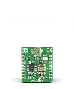

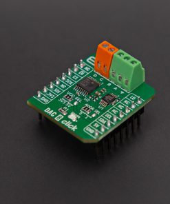
DAC 8 Click
R960.00 ex. VAT
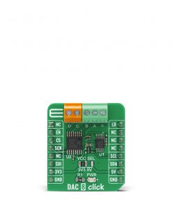
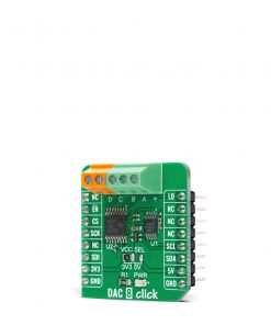
DAC 8 Click is a compact add-on board that contains a fully-featured, general-purpose voltage-output digital-to-analog converter. This board features the DAC8554IPWR, a 16-bit QUAD channel voltage-output digital to analog converter from Texas Instruments. It offers the low-power operation, good linearity, exceptionally low glitch, and supports a 3-wire SPI serial interface with a clock rate up to 50MHz. Requires an external reference voltage provided by I2C compatible DAC60501MDGSR to set the output range of each DAC channel. It has many features that make it attractive for various applications such as battery-operated equipment, digital gain and offset adjustment, programmable voltage and current sources, and many more.
DAC 8 Click is supported by a mikroSDK compliant library, which includes functions that simplify software development. This Click board™ comes as a fully tested product, ready to be used on a system equipped with the mikroBUS™ socket.
Stock: Lead-time applicable.
| 5+ | R912.00 |
| 10+ | R864.00 |
| 15+ | R816.00 |
| 20+ | R785.28 |
How does it work?
DAC 8 Click is based on the DAC8554IPWR, a 16-bit QUAD channel, ultra-low glitch, voltage-output digital to analog converter from Texas Instruments. It offers good linearity, exceptionally low glitch, and it has high precision output amplifier that allows rail-to-rail output swing over a wide range of supply voltage. What this component additionally has is a Power-On reset function, which ensures that DAC outputs power-up at zero-scale and remains there until a proper write operation occurs. Also, it provides a power-down feature that reduces the current consumption to 175nA per channel.

To achieve a fully flexible range of the DAC8554IPWR, an external voltage reference is made user-programmable. For this purpose, the Click board™ uses another DAC, DAC60501MDGSR, 12-bit DAC from Texas Instruments, whose output is brought to the VREF pin of the DAC8554IPWR. That way, the reference voltage of the DAC8554IPWR can be set at any value between 0V and 5V, provides high precision and low power consumption as well. That makes the DAC 8 Click fully customizable solution, well suited for applications where the maximum precision from the output 16-bit DAC is needed. DAC60501MDGSR uses the I2C serial interface to communicate with the MCU and operates at clock rate up to 100kHz, with selectable I2C address through ADDR SEL jumper.
The DAC 6 Click communicates with MCU using the 3-Wire SPI serial interface that is compatible with standard SPI, QSPI™, MICROWIRE™ and operates at clock rates up to 50 MHz. Additional functionality such as software simultaneous update capability is implemented and routed at the PWM pin of the mikroBUS™, which allows when new data enter the device, all of DAC outputs can be updated simultaneously and synchronously with the clock. It also possesses enable function routed at CS pin of the mikroBUS™ that is used to connect the SPI interface to the serial port.
This Click Board™ is designed to be operated with both 3.3V and 5V logic levels. The onboard SMD jumper labeled as VCC SEL allows voltage selection for interfacing with both 3.3V and 5V MCUs. More information about the DAC8554IPWR’s functionality, electrical specifications, and typical performance can be found in the attached datasheet. However, the Click board™ comes equipped with a library that contains easy-to-use functions, and a usage example that can be used as a reference for the development.
Specifications
Type
DAC
Applications
Can be used in battery-operated equipment, digital gain and offset adjustment, programmable voltage and current sources, and many more.
On-board modules
DAC 8 Click is based on the DAC8554IPWR, a 16-bit QUAD channel, ultra-low glitch, voltage-output digital to analog converter from Texas Instruments.
Key Features
Low power consumption, high precission, ultra-low glitch, rail-to-rail voltage output, accuracy, stability, and more.
Interface
GPIO,I2C,SPI
Feature
No ClickID
Compatibility
mikroBUS™
Click board size
S (28.6 x 25.4 mm)
Input Voltage
3.3V or 5V
Pinout diagram
This table shows how the pinout on DAC Click corresponds to the pinout on the mikroBUS™ socket (the latter shown in the two middle columns).
| Notes | Pin | Pin | Notes | ||||
|---|---|---|---|---|---|---|---|
| NC | 1 | AN | PWM | 16 | LD | Software Update | |
| SPI Enable | EN | 2 | RST | INT | 15 | NC | |
| SPI Chip Select | CS | 3 | CS | RX | 14 | NC | |
| SPI Clock | SCK | 4 | SCK | TX | 13 | NC | |
| SPI Data OUT | SDO | 5 | MISO | SCL | 12 | SCL | I2C Clock |
| SPI Data IN | SDI | 6 | MOSI | SDA | 11 | SDA | I2C Data |
| Power Supply | 3.3V | 7 | 3.3V | 5V | 10 | 5V | Power Supply |
| Ground | GND | 8 | GND | GND | 9 | GND | Ground |
Onboard settings and indicators
| Label | Name | Default | Description |
|---|---|---|---|
| LD1 | PWR | – | Power LED Indicator |
| JP1 | VCC SEL | Left | Power Supply Voltage Selection 3V3/5V: Left position 3V3, Right position 5V |
DAC 8 Click electrical specifications
| Description | Min | Typ | Max | Unit |
|---|---|---|---|---|
| Supply Voltage | -0.3 | – | 6 | V |
| Maximum Current Consumption | – | – | 208 | μA |
| SPI Clock Frequency | – | – | 50 | MHz |
| Operating Temperature Range | -40 | – | +105 | °C |
Software Support
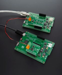
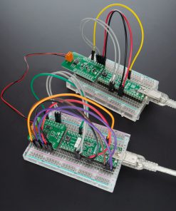
DAC 8 Click demo application is developed using the NECTO Studio, ensuring compatibility with mikroSDK‘s open-source libraries and tools. Designed for plug-and-play implementation and testing, the demo is fully compatible with all development, starter, and mikromedia boards featuring a mikroBUS™ socket.
Example Description
This Click carries 12-bit buffered Digital-to-Analog Converter. It converts digital value to the corresponding voltage level using external voltage reference.
Key Functions
dac8_cfg_setupConfig Object Initialization function.dac8_initInitialization function.dac8_device_configoutput digital-to-analog converter on DAC 8 Click board.dac8_load_dacbuffers of all channels must be loaded with desired data before call Load DAC function.dac8_set_vrefWith Precision Internal Reference on DAC 8 Click board.
Application Init
Initialization driver enables – I2C. Configure DAC60501: executes call software reset, disable sync and internal reference and disable Power-down mode, the set reference voltage is internally divided by a factor of 2, amplifier for corresponding DAC has a gain of 2. Initialization driver enables – SPI, enable DAC8554, also write log.
Application Task
This is an example that demonstrates the use of the DAC 8 Click board. DAC 8 board changeing output values: Channel A ~ 2500 mV, Channel B ~ 1250 mV, Channel C ~ 625 mV, Channel D ~ 312 mV. All data logs write on USB uart changes every 5 sec.
Application Output
This Click board can be interfaced and monitored in two ways:
- Application Output – Use the “Application Output” window in Debug mode for real-time data monitoring. Set it up properly by following this tutorial.
- UART Terminal – Monitor data via the UART Terminal using a USB to UART converter. For detailed instructions, check out this tutorial.
Additional Notes and Information
The complete application code and a ready-to-use project are available through the NECTO Studio Package Manager for direct installation in the NECTO Studio. The application code can also be found on the MIKROE GitHub account.
Resources
Downloads
| Weight | 19 g |
|---|---|
| Brand | MikroElektronika |