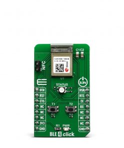
How does it work?
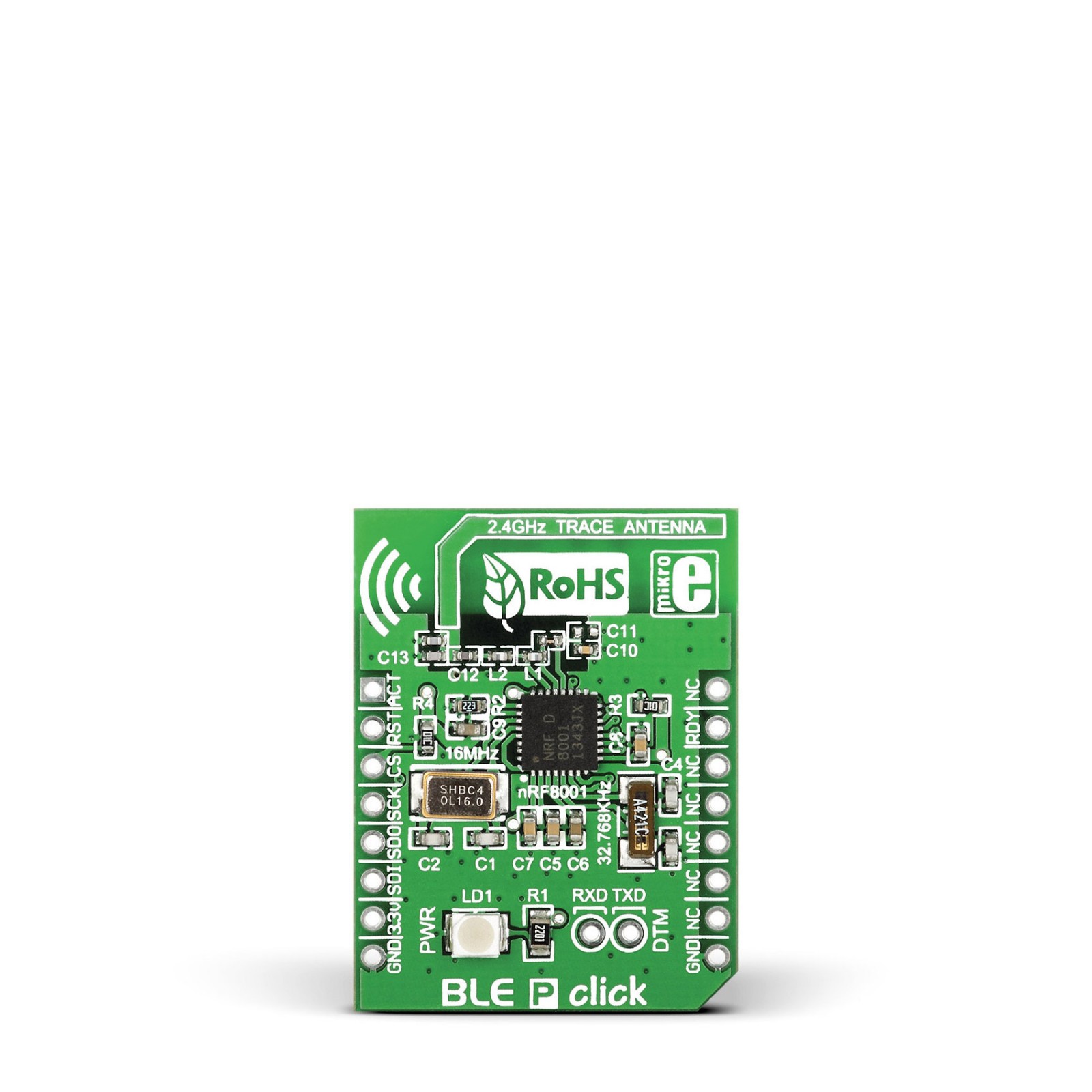
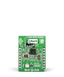
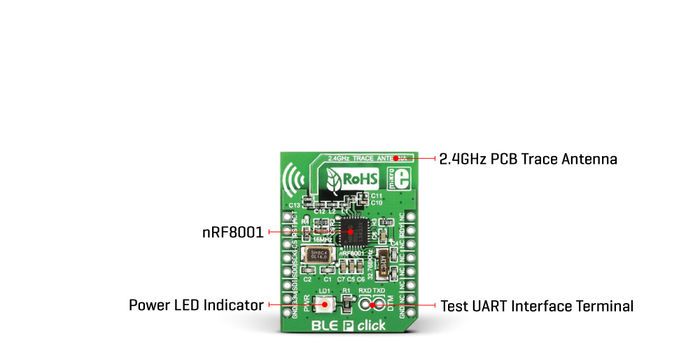
BLE P Click is based on the nRF8001, a Bluetooth 4.0 transceiver from Nordic Semiconductor. The nRF8001 has an on-chip non-volatile memory for storing service configuration used through an integrated Application Controller Interface (ACI), a logical interface between this IC and the application. This storage is used to select and combine the necessary services, thus reducing the application’s requirements on the host MCU for handling the real-time operations of the Bluetooth low-energy communication protocol. In addition, the nRF8001 includes a power supply voltage monitor and temperature sensor that further reduces the requirements of the application controller and, thus, the number of the board’s components.
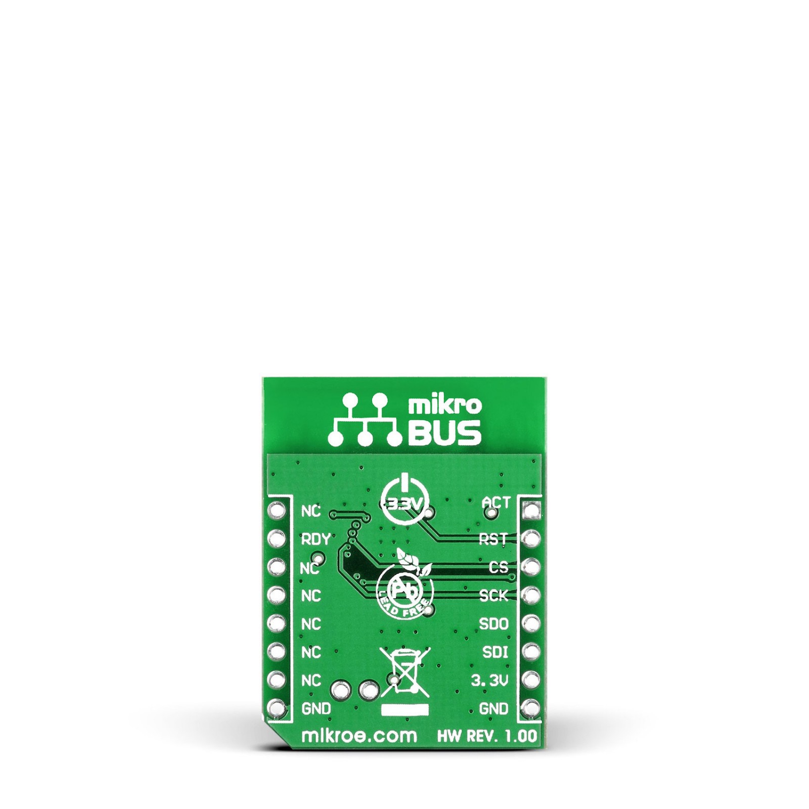
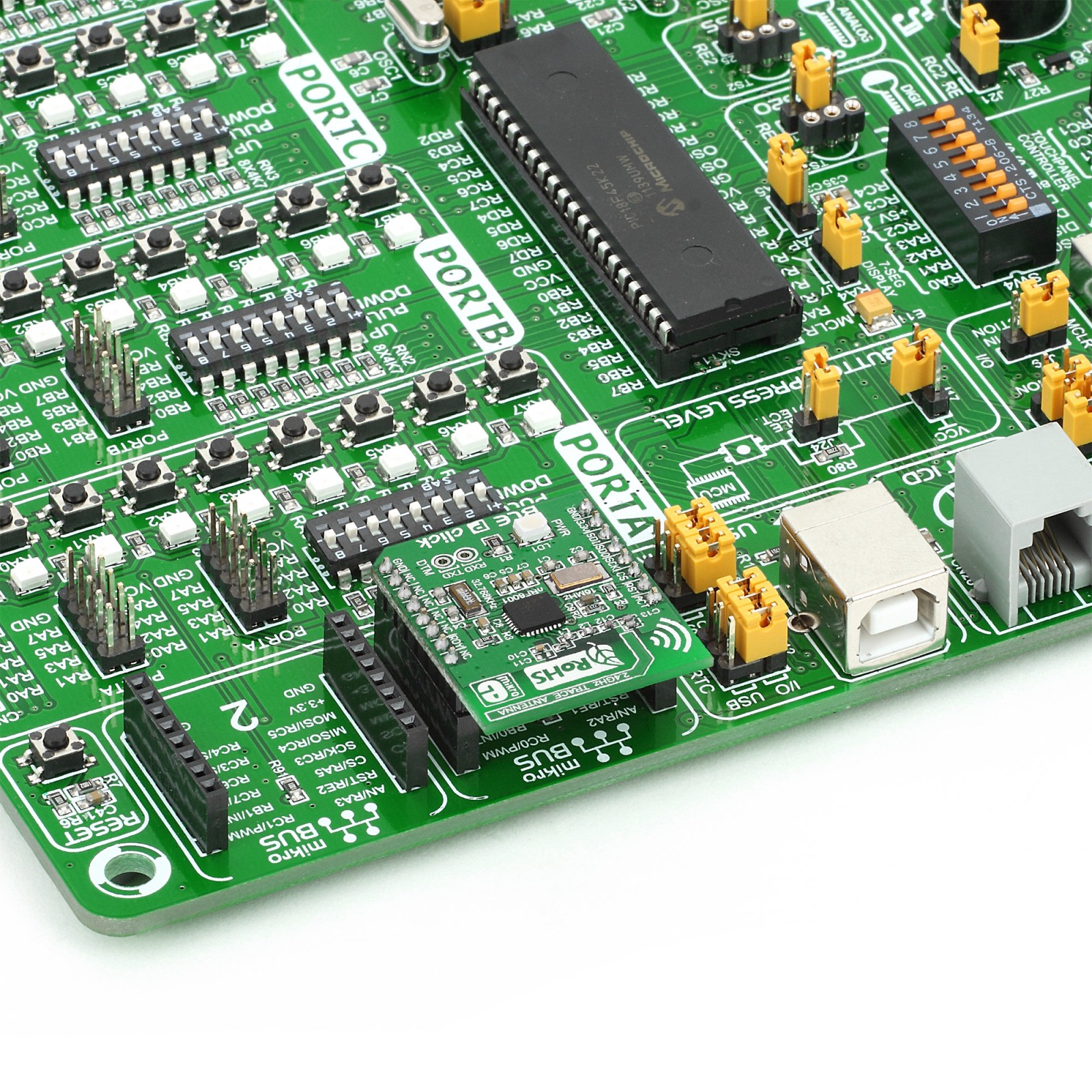
BLE P Click uses a standard SPI serial interface to establish communication between ACI and the host MCU over the mikroBUS™ socket. The nRF8001 can receive new data over the air at any time, but it can also be busy processing connection events or new data. For the best possible indication of this state, beside an SPI CS pin, there is an RDY pin that serves as an ACI-ready indication (handshaking, active low). This Click board™ also features an RST pin for resetting the nRF8001 and an ACT pin, an optional output signal (ACTIVE) activated before the radio becomes active. This timing signal enables controlling the peak current drain of your application, avoiding overload of the power supply, thus making this Click board™ a perfect solution for projects that require work on small battery capacity. A separate UART interface on RXS/TXD pins of unpopulated terminal gives access to the Bluetooth low energy Direct Test Mode (DTM), allowing testing RF parameters of the BLE P Click’s radio design.
If you want to get started with BLE, check out our BLE Android app that works on all devices with hardware and software support for BLE. All you have to do is to make sure you use it on Android devices.
This Click board™ can be operated only with a 3.3V logic voltage level. The board must perform appropriate logic voltage level conversion before using MCUs with different logic levels. However, the Click board™ comes equipped with a library containing functions and an example code that can be used, as a reference, for further development.
Specifications
Type
BT/BLE
Applications
Can be used for general data transmission applications such as thermometers, blood pressure monitors, weight scales, toys, pet supplies, IoT sensor nodes, and more
On-board modules
nRF8001 – Bluetooth 4.0 transceiver from Nordic Semiconductor
Key Features
Low power consumption, BLE PHY, link layer features, GAP features, main SPI interface, an additional UART pins (RXD/TXD) for Direct Test Mode interface, RF activity indicator, security manager, and more
Interface
GPIO,SPI
Feature
No ClickID
Compatibility
mikroBUS™
Click board size
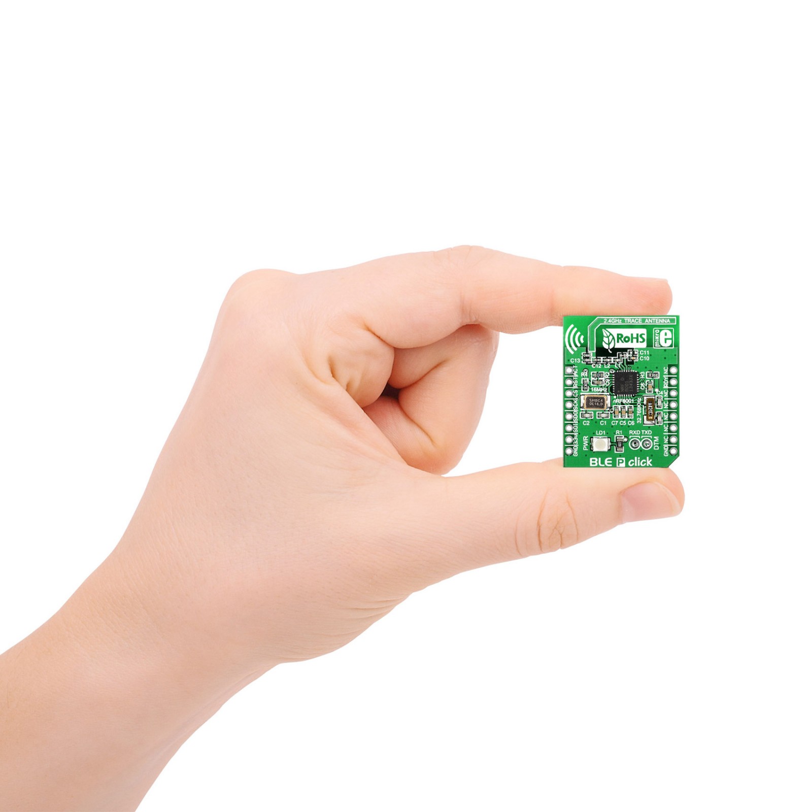
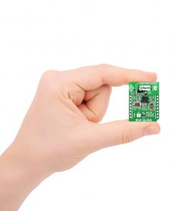
S (28.6 x 25.4 mm)
Input Voltage
3.3V
Pinout diagram
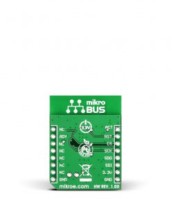
This table shows how the pinout on BLE P Click corresponds to the pinout on the mikroBUS™ socket (the latter shown in the two middle columns).
Onboard settings and indicators
Label | Name | Default | Description |
---|---|---|---|
LD1 | PWR | – | Power LED Indicator |
BLE P Click electrical specifications
Description | Min | Typ | Max | Unit |
---|---|---|---|---|
Supply Voltage | – | 3.3 | – | V |
Operating Frequency Range | 2402 | – | 2480 | MHz |
On-air Data Rate | – | 1 | – | Mbps |