8×8 G Click
R465.00 ex. VAT
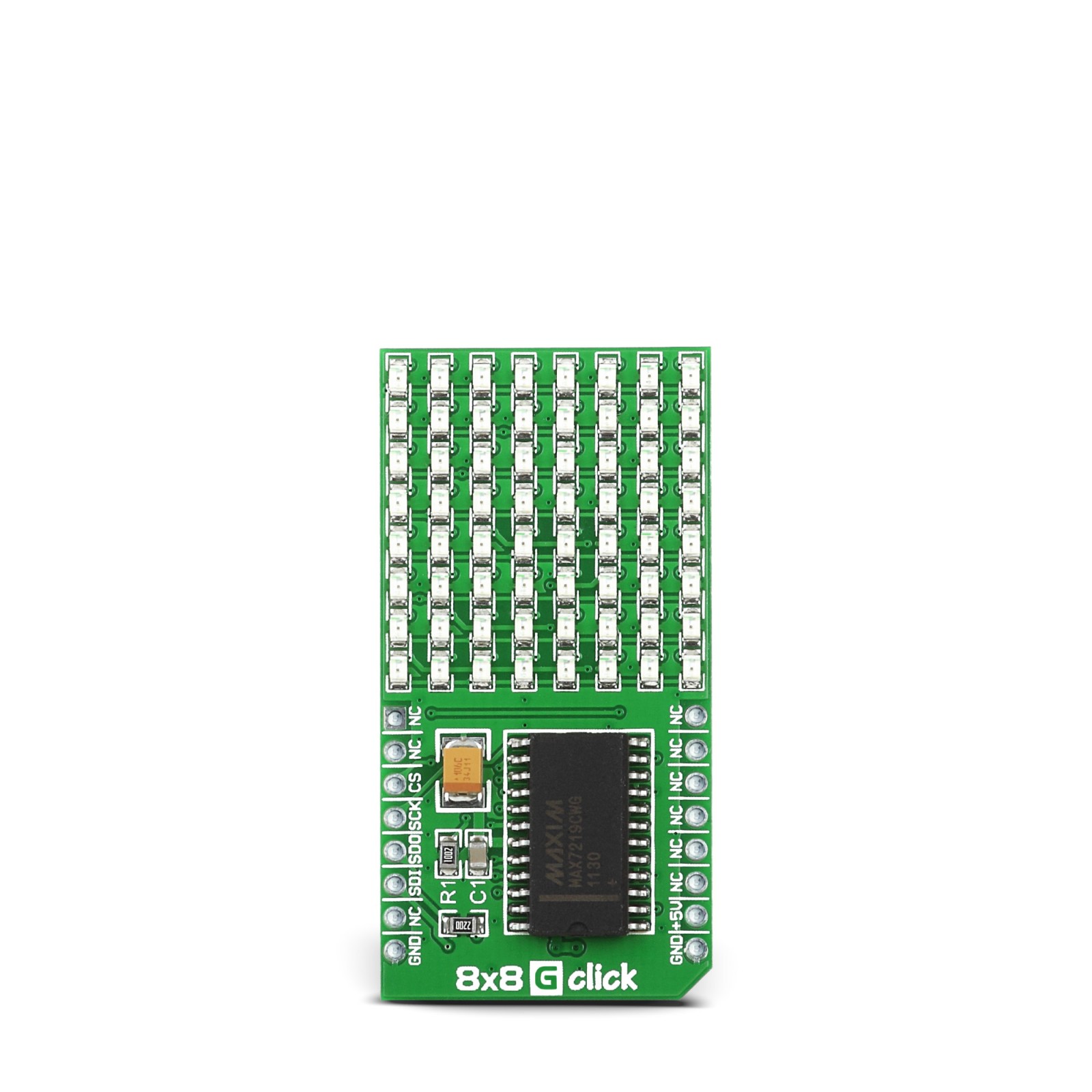
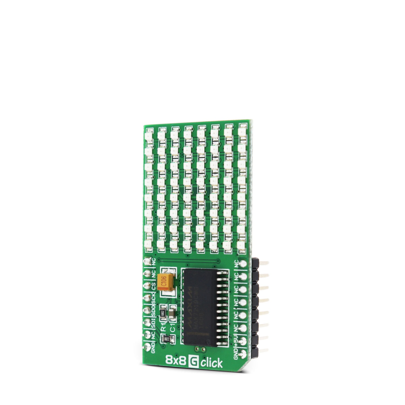
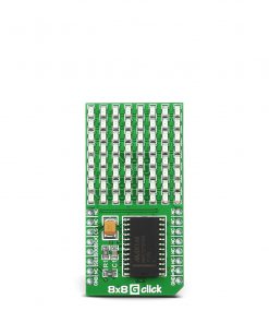
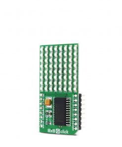
8×8 G click is a 64 LED matrix display Click board™, composed of SMD LEDs organized in 8 rows by 8 columns. It has a digital brightness control in 16 steps, it can control every LED in the display matrix independently, it blanks the display on power up to eliminate glitches and it requires a single resistor to control the current through all the LEDs at once, which simplifies the design. 8×8 G click uses a fast SPI communication protocol, allowing fast display response and no lag.
Stock: Lead-time applicable.
| 5+ | R441.75 |
| 10+ | R418.50 |
| 15+ | R395.25 |
| 20+ | R380.37 |
8×8 G click is a 64 LED matrix display Click board™, composed of SMD LEDs organized in 8 rows by 8 columns. It has a digital brightness control in 16 steps, it can control every LED in the display matrix independently, it blanks the display on power up to eliminate glitches and it requires a single resistor to control the current through all the LEDs at once, which simplifies the design. 8×8 G click uses a fast SPI communication protocol, allowing fast display response and no lag.
8×8 G click can be used as a display or signalization output for a range of applications that are designed to display various information or graphics on the matrix LED display. By using functions provided by MikroElektronika, it is possible to make a text scroller in a very simple way, greatly expanding the functionality of the 8×8 click.
How does it work?
The main active component of the 8×8 click is the MAX7129, a serially interfaced, a common cathode 8-digit LED display driver from Analog Devices. It consists of 8×8 RAM cells for storing the digit data, 16bit data shifter, constant current source for the LED segments, address register decoder, the intensity pulse width modulator, the digit scan section and finally output LED drivers. This IC is primarily designed to drive eight 7-segment LED digits with an additional dot segment (8 digits by 8 segments), but it can be used to drive a set of similar types of displays, such as LED matrices (e.g. 8×8 click), bar graph displays, panel meters, and similar. For that reason, the output drivers are referred to as digit outputs and segment outputs. This categorization also mirrors the way the internal memory is organized. The scan rate of the LED matrix display is 800Hz, typically.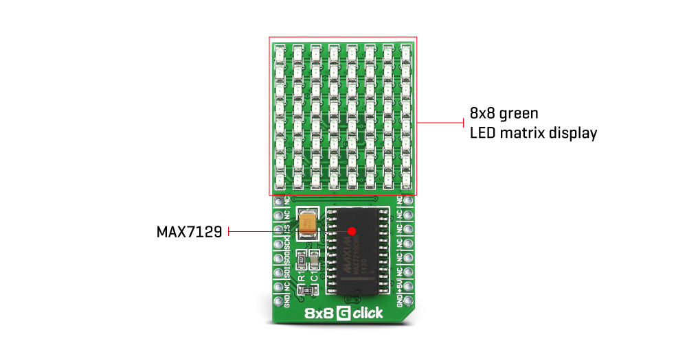
The communication is done via the SPI interface. The data is sent by the host MCU, through the DIN pin of the MAX7129 IC, in packets that are 16 bits wide. A serial clock signal should be present at the CLK pin of this IC, and its frequency should stay below 10MHz. The DIN and CLK pins are routed to the mikroBUS™ SCK and MOSI pins so that it can be easily connected to the SPI bus of the host MCU. DOUT pin can be used to daisy-chain several devices. The data from DIN pin is mirrored on the DOUT pin, but with the delay of 16.5 clock cycles. This pin is routed to the mikroBUS™ MISO pin. Unlike the regular SPI, this IC allows clocking the data in, regardless of the LOAD pin. However, the internal 16bit shift register will shift the data only on a rising edge of the LOAD pin, which needs to happen on the 16th rising edge, and before the 17th rising edge of the clock signal – else, the current data is discarded, and the shift register expects a new 16bit data packet to be clocked in. The LOAD pin is routed to the CS pin of the mikroBUS™
The input data is clocked in as described above, in a form of 16bit packets. Those packets contain the command and the data, both interleaved inside the packet. The first 8 bits are the data bits (D0 to D7), while the next four bits contain the register address (D8 to D11). The last four bits are disregarded by the internal logic (D12 to D15). The data is clocked MSB first, so the first received bit would be D15.
There is a number of various registers embedded in the MAX7129 IC that are used to perform a range of different functions. It has registers to set modes for each digit, setting it to binary coded decimal format (BCD) or no coding at all. It has a scan limit register, which limits display scanning to an arbitrary number of digits, test register which sets all the segments on all the digits to be fully ON, registers that allow intensity control by changing the duty cycle of the PWM, and so on. It should be noted that some of the registers make sense only if used with 7-segment LED elements, so their use should be avoided completely in the code, as the 8×8 click board is designed as a matrix LED display. More information about the registers and their usage can be found in the MAX7129 datasheet. Using functions provided by MikroElektronika ensures that the correct registers are accessed and exposes a comprehensive set of commands to work with the 8×8 G click.
An onboard resistor sets the peak current through the segments. This current is fine-tuned according to used LEDs requirements. The brightness can be changed by writing data in the intensity register. The lower 4 nibbles of this register are used to control the internal PWM duty cycle, allowing brightness control in 16 steps. This intensity register affects the global brightness, so it is used to dim the entire display at once.
Specifications
Type
LED Matrix
Applications
8×8 G click brings serial 8×8 Green LED display matrix to your design
On-board modules
MAX7219 8-digit LED display driver
Key Features
On-chip BCD code-B decoder with 8×8 area
Interface
SPI
Feature
No ClickID
Compatibility
mikroBUS™
Click board size
M (42.9 x 25.4 mm)
Input Voltage
5V
Pinout diagram
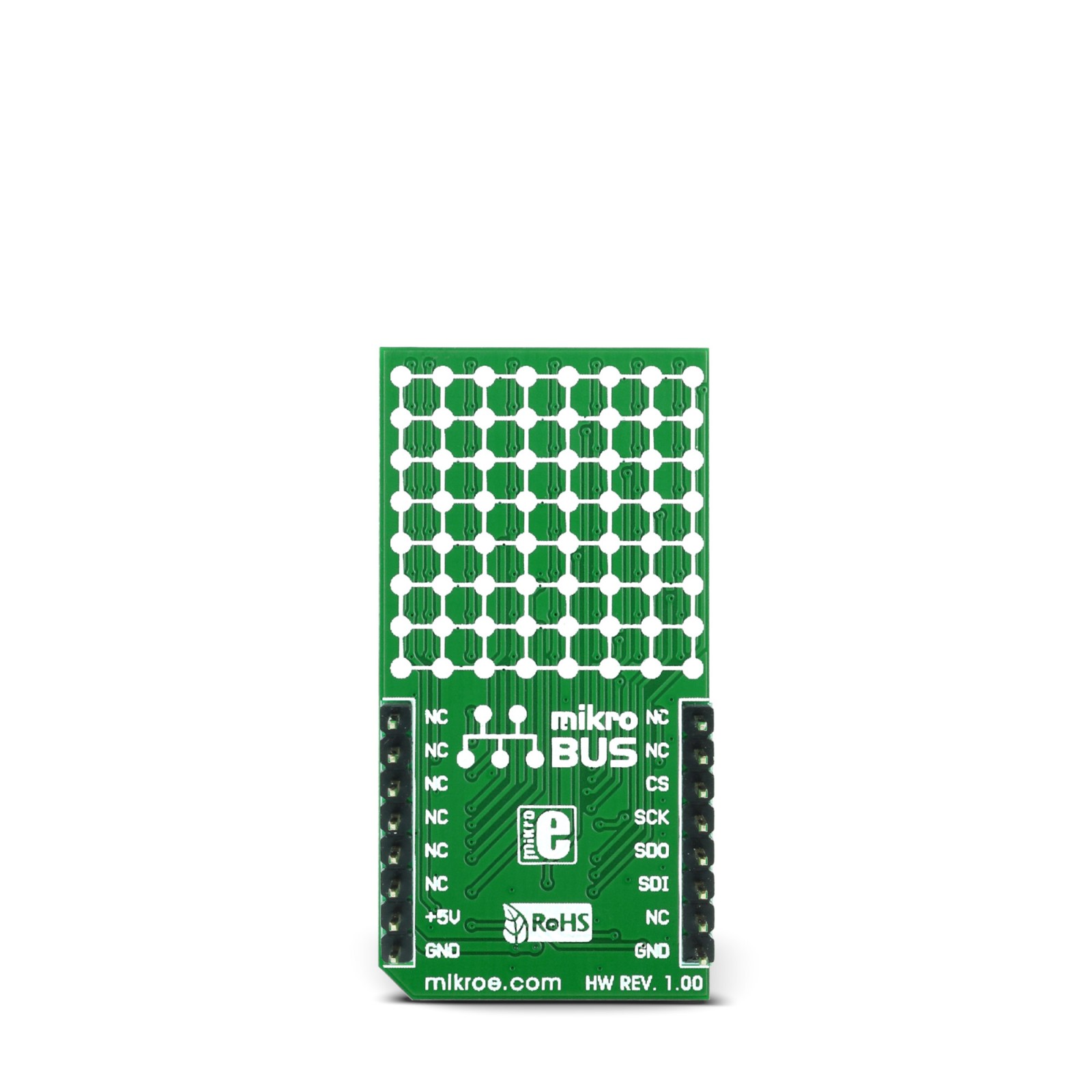
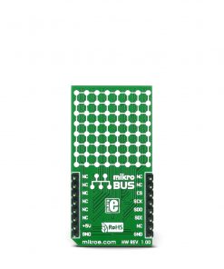
This table shows how the pinout on 8×8 G click corresponds to the pinout on the mikroBUS™ socket (the latter shown in the two middle columns).
Software support
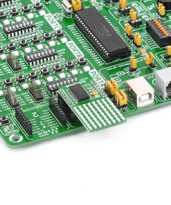
We provide a library for 8×8 G click on our LibStock page, as well as a demo application (example), developed using MikroElektronika compilers and mikroSDK. The provided click library is mikroSDK standard compliant. The demo application can run on all the main MikroElektronika development boards.
Library Description
The library provides generic functions for controlling the Click board™.
Key functions:
void c8x8g_writeReg(uint8_t Reg, uint8_t Value);- Function for writing data to a register.void c8x8g_writeText(uint8_t *pStr, uint8_t nLenght);- Scrolls provided text.
Examples Description
The application is composed of three sections:
- System Initialization – Initializes CS pin as output and SPI module
- Application Initialization – Driver initialization and default configuration of the 8×8 click board.
- Application Task – (code snippet) – Sequential writing of provided string each one second.
void applicationTask()
{
 c8x8b_displayWord(&demoString[0]);
 Delay_1sec();
}
The full application code, and ready to use projects can be found on our LibStock page.
Other mikroE Libraries used in the example:
- Conversions Library
- C_String Library
- SPI Library
Additional notes and information
Depending on the development board you are using, you may need USB UART click, USB UART 2 click or RS232 click to connect to your PC, for development systems with no UART to USB interface available on the board. The terminal available in all MikroElektronika compilers, or any other terminal application of your choice, can be used to read the message.
mikroSDK
This click board is supported with mikroSDK - MikroElektronika Software Development Kit. To ensure proper operation of mikroSDK compliant click board demo applications, mikroSDK should be downloaded from the LibStock and installed for the compiler you are using.
For more information about mikroSDK, visit the official page.
Resources
Downloads
| Weight | 32 g |
|---|---|
| Brand | MikroElektronika |

