How does it work?
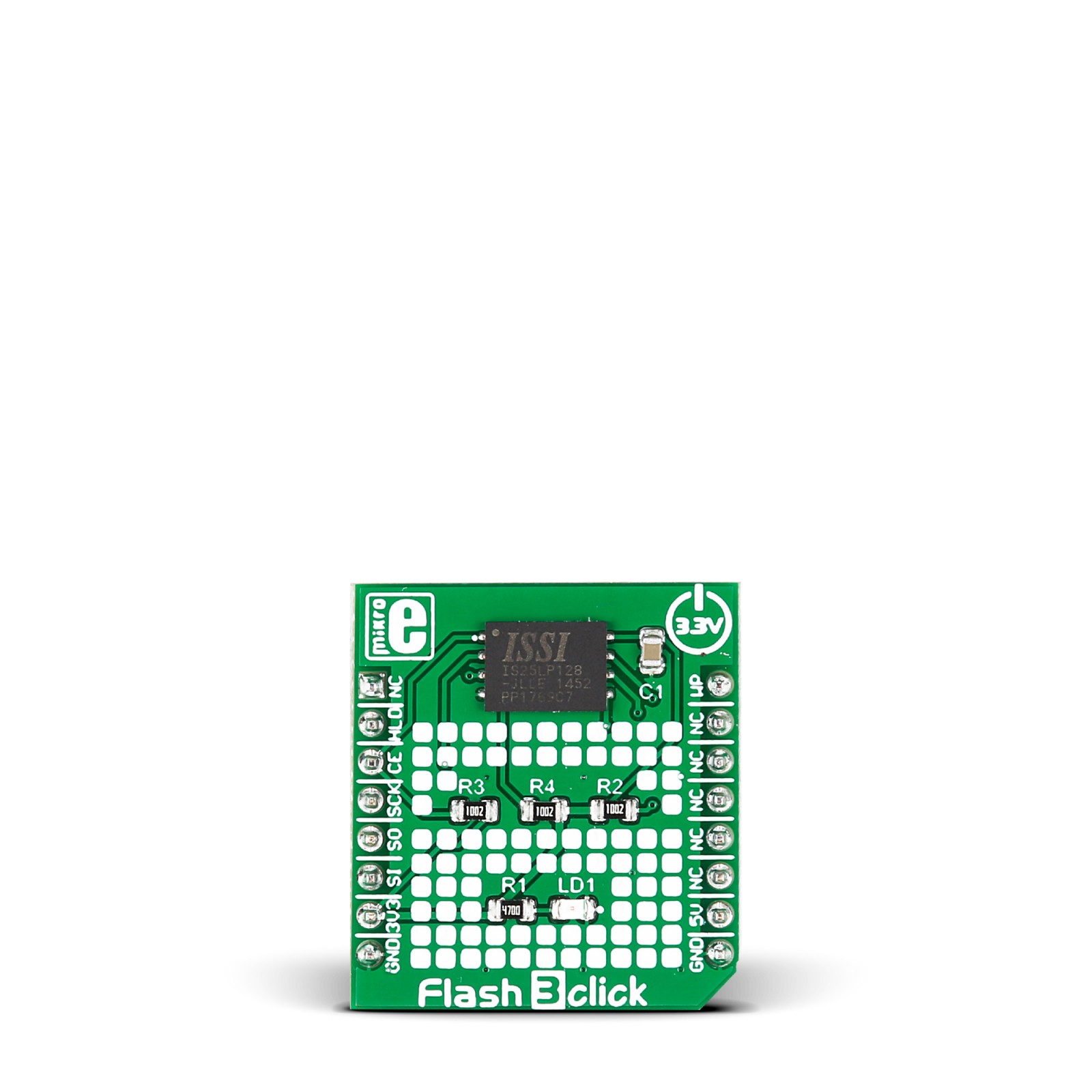
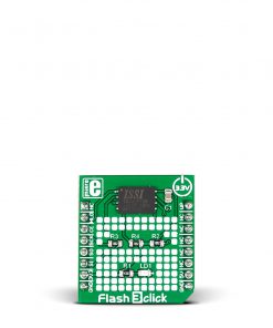
Flash 3 Click is based on the IS25LP128, a serial Flash memory with 133MHz multi I/O SPI & quad I/O QPI DTR interfaces from Integrated Silicon Solution. This Flash memory chip supports Serial Flash Discoverable Parameters (SFDP), selectable dummy cycles, SPI modes 0 and 3, and configurable drive strength. The flexible and efficient memory architecture allows chip erase with uniform sector/block erase (4/32/64 KB) and program/erase suspend and resume. The read and program modes consist of low instruction overhead operations, continuous read 8/16/32/64-byte burst wrap, selectable burst length, and more. There are software and hardware protections, power supply lock protection, a 4×256-byte dedicated security area with OTP user-lockable bits, and the 128-bit Unique ID for each device.
The Flash 3 Click communicates with the host MCU through an industry-standard SPI serial interface, supporting the two most common SPI modes, SPI Mode 0 and 3, with a maximum frequency of 133MHz in Fast Read mode. The Flash 3 Click features write-protect ability over the WP pin, with active LOW. The HLD pin is a communication hold pin, and the Flash memory can stay in a hold state with logic LOW, in which time the device is paused without resetting the serial sequence. The CE pin enables and disables the device’s operation on this Click board™, pulled high for normal operation.
This Click board™ can only be operated with a 3.3V logic voltage level. The board must perform appropriate logic voltage level conversion before using MCUs with different logic levels. However, the Click board™ comes equipped with a library containing functions and an example code that can be used, as a reference, for further development.
Specifications
Type
FLASH
Applications
Can be used for the development of applications for storage and data transfer in consumer devices, and industrial applications
On-board modules
IS25LP128 – serial Flash memory from Integrated Silicon Solution
Key Features
128-bit unique ID, Standard/Dual/Quad SPI, high speed clock frequency, protection features, reliability, enhanced access performance, low power consumption, and more
Interface
GPIO,SPI
Feature
No ClickID
Compatibility
mikroBUS™
Click board size
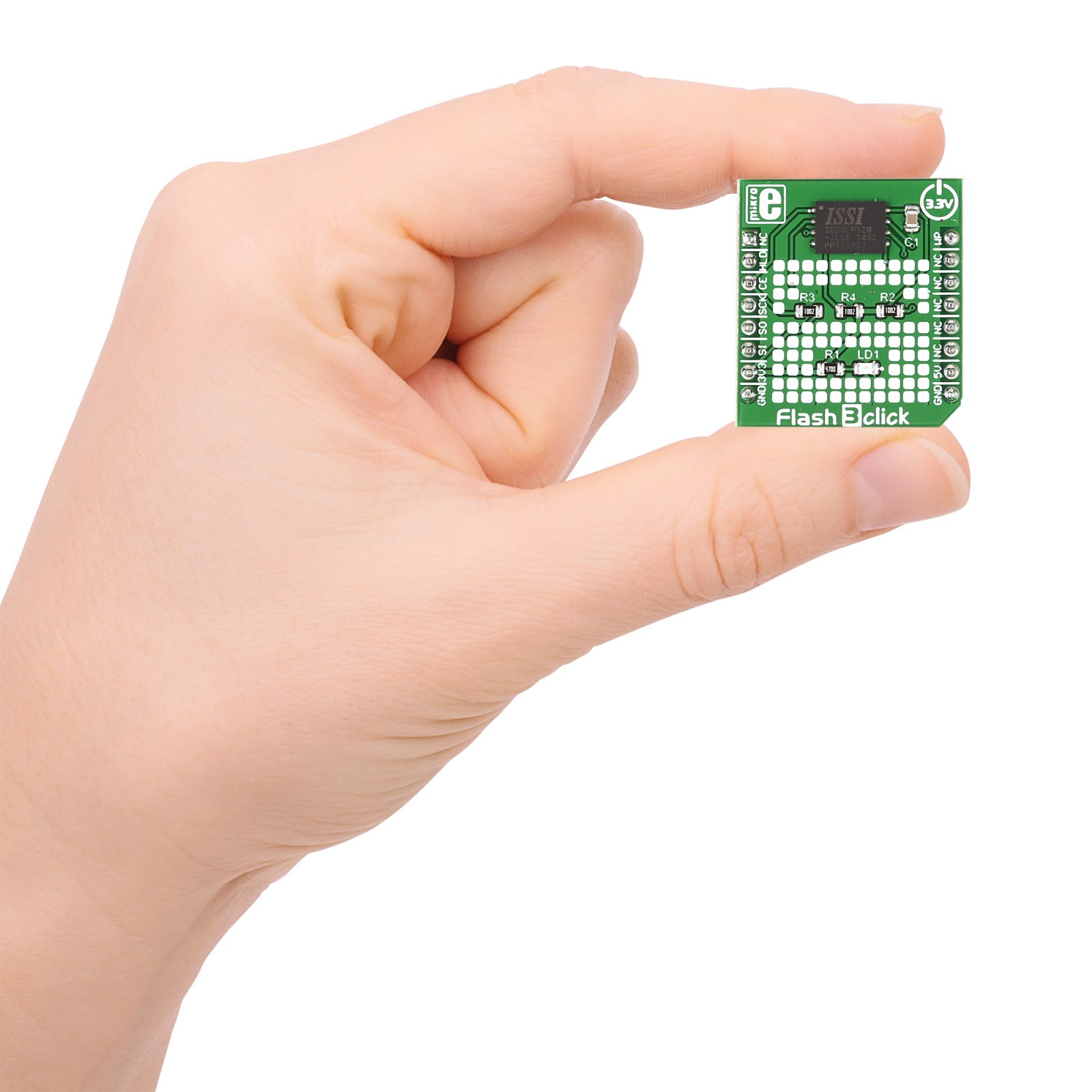
S (28.6 x 25.4 mm)
Input Voltage
3.3V,5V
Pinout diagram
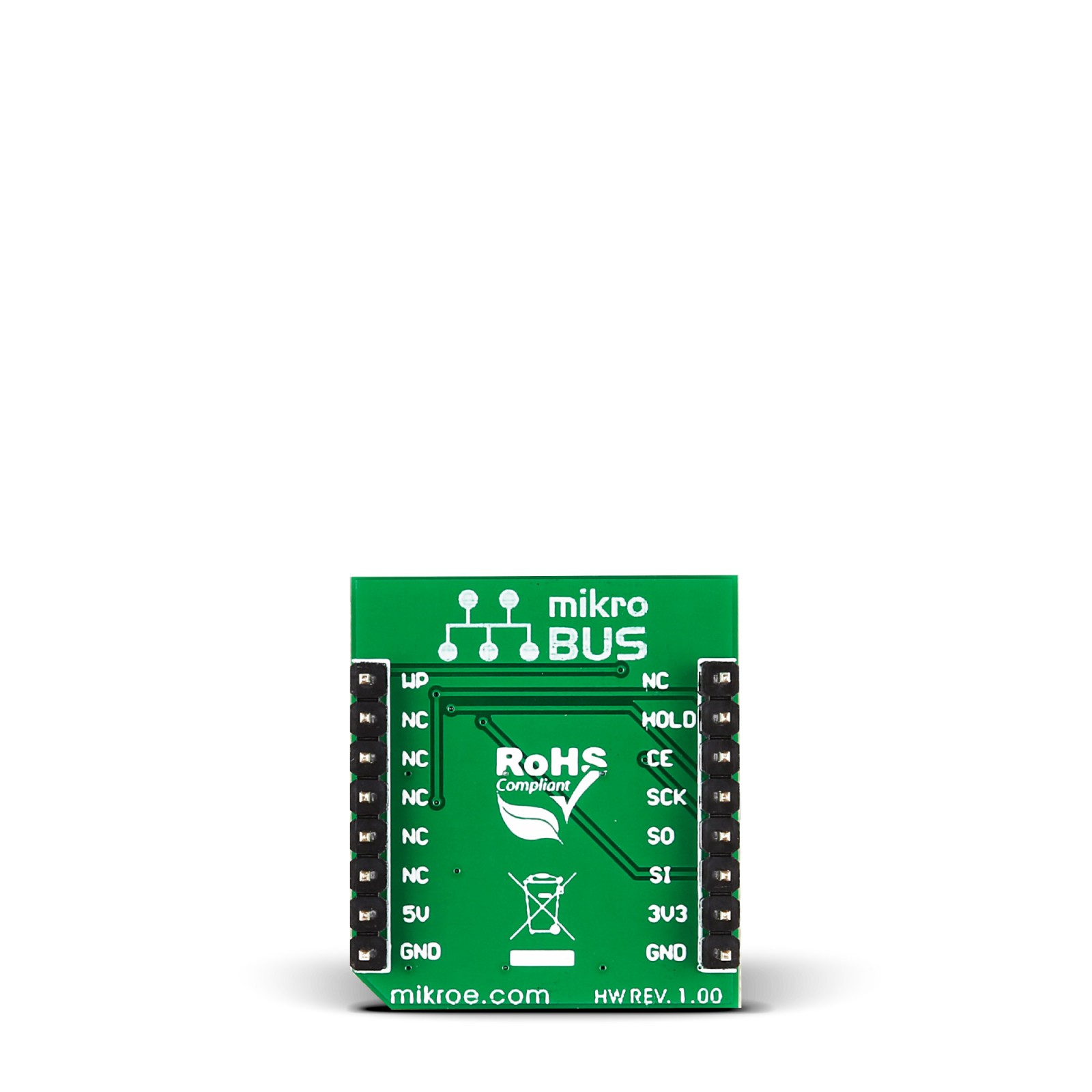
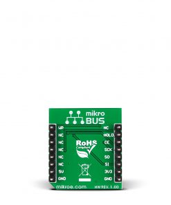
This table shows how the pinout on Flash 3 Click corresponds to the pinout on the mikroBUS™ socket (the latter shown in the two middle columns).
Onboard settings and indicators
Label | Name | Default | Description |
---|---|---|---|
LD1 | PWR | – | Power LED Indicator |
Flash 3 Click electrical specifications
Description | Min | Typ | Max | Unit |
---|---|---|---|---|
Supply Voltage | – | 3.3 | – | V |
Memory Size | – | – | 128 | Mbit |
Organization | 16M x 8 | |||
Write Endurance | 100k | – | – | Cycles |
Data Retention | 20 | – | – | Years |
Software Support
We provide a library for the Flash 3 Click as well as a demo application (example), developed using MIKROE compilers. The demo can run on all the main MIKROE development boards.
Package can be downloaded/installed directly from NECTO Studio Package Manager (recommended), downloaded from our LibStock™ or found on Mikroe github account.
Library Description
This library contains API for Flash 3 Click driver.
Key functions
-
Pause function.
-
Unpause function.
-
Unpause function.
Example Description
This applicaion adding more flash memory.
void application_task ( void )
{
char val_in[ 8 ] = { 0x4D, 0x49, 0x4B, 0x52, 0x4F, 0x45, 0x00 };
char val_out[ 8 ] = { 0 };
log_printf( &logger, "rn ____________________ rn" );
log_printf( &logger, "Begin demonstration! rnrn" );
log_printf( &logger, "Writing : %srn", val_in );
flash3_write( &flash3, 0x000000, &val_in[ 0 ], 6 );
Delay_ms( 100 );
log_printf( &logger, "------------------ rn" );
log_printf( &logger, "Reading : %srn", val_in );
flash3_normal_read( &flash3, 0x000000, &val_in[ 0 ], 6 );
Delay_ms( 100 );
log_printf( &logger, "------------------ rn" );
log_printf( &logger, "Erasing... rn" );
flash3_sector_erase( &flash3, 0x000000 );
Delay_ms( 300 );
log_printf( &logger, "Erased!" );
Delay_ms( 100 );
log_printf( &logger, "------------------ rn" );
log_printf( &logger, "Reading : %srn", val_out );
flash3_fast_read( &flash3, 0x000000, &val_out[ 0 ], 6 );
Delay_ms( 100 );
log_printf( &logger, "------------------ rn" );
log_printf( &logger, "Demonstration over!" );
log_printf( &logger, "rn ___________________ rn" );
Delay_ms( 5000 );
}
The full application code, and ready to use projects can be installed directly from NECTO Studio Package Manager (recommended), downloaded from our LibStock™ or found on Mikroe github account.
Other Mikroe Libraries used in the example:
- MikroSDK.Board
- MikroSDK.Log
- Click.Flash3
Additional notes and informations
Depending on the development board you are using, you may need USB UART click, USB UART 2 Click or RS232 Click to connect to your PC, for development systems with no UART to USB interface available on the board. UART terminal is available in all MIKROE compilers.
mikroSDK
This Click board™ is supported with mikroSDK – MIKROE Software Development Kit. To ensure proper operation of mikroSDK compliant Click board™ demo applications, mikroSDK should be downloaded from the LibStock and installed for the compiler you are using.
For more information about mikroSDK, visit the official page.