How does it work?
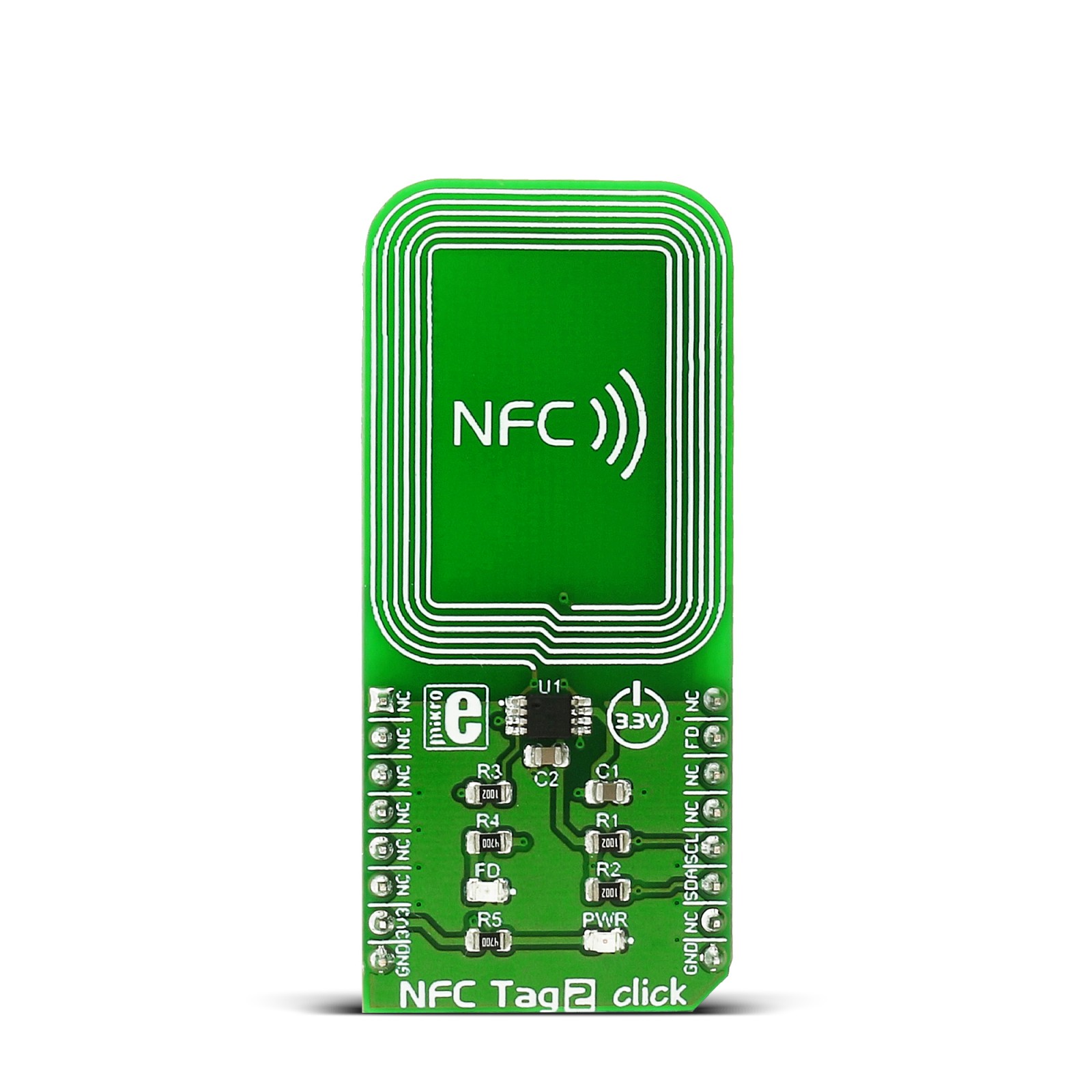
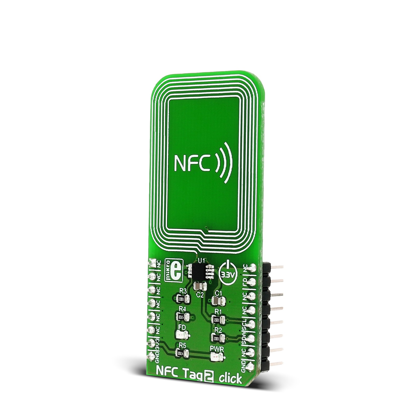
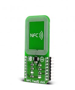
NFC Tag 2 Click is based on the NT3H2111, an energy-harvesting NFC Forum Type 2 tag from NXP. It is ISO/IEC 14443 Part 2 and 3 compliant and features the unique 7-byte UID. The NFC IC transfers data in pass-through mode with a 64-byte SRAM buffer or using FAST_WRITE and FAST_READ NFC commands for higher data throughput. The security and memory-access management features NFC silence to turn off the NFC interface, signature based on Elliptic Curve Cryptography (ECC), full, read-only, or no memory access from the I2C interface, and full, read-only, or no memory access from the NFC interface based on a 32-bit password. The power management part of the NFC IC features the configurable field-detection output signal for data-transfer synchronization device wake-up and energy harvesting from the NFC field. The energy harvesting allows for powering external devices such as the host MCU. It could typically provide a 5mA at 2V.
The NGC Tag 2 Click can achieve up to 106kbps of contactless transmission data over the onboard printed NFC antenna. The antenna operates at 13.56MHz. It benefits from full interoperability with every NFC-enabled device. The NFC State Machine consists of the Idle, Ready 1 and 2, Active, Authenticated, and Halt states. Those states depend on the mode of operation.
NFC Tag 2 Click uses a standard 2-Wire I2C interface to communicate with the host MCU, supporting fast mode and SCL frequency of up to 400KHz. The NFC tag uses an FD pin for field detection to indicate to the host MCU that the data is ready to be read from the SRAM. The NFC Tag 2 Click has an FD LED to represent the energy-harvested power visually.
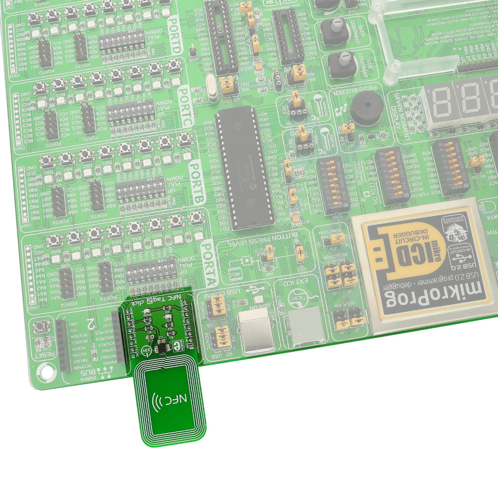
This Click board™ can be operated only with a 3.3V logic voltage level. The board must perform appropriate logic voltage level conversion before using MCUs with different logic levels. However, the Click board™ comes equipped with a library containing functions and an example code that can be used as a reference for further development.
Specifications
Type
RFID/NFC
Applications
Can be used for the development of home automation, consumer applications, fitness equipment, meters, electronic shelf labels, and more
On-board modules
NT3H2111 – energy-harvesting NFC Forum Type 2 tag from NXP
Key Features
Energy harvesting, the NFC Tag can provide typically 5mA at 2V for powering up the host MCU, built-in printed antenna, unique 7-byte UID, contactless data transmission, built-in EEPROM and SRAM, field programmable read-only locking function, 32-bit password protection, pass-through and mirror mode, fully interoperable with every NFC-enabled device, and more
Interface
I2C
Feature
No ClickID
Compatibility
mikroBUS™
Click board size
L (57.15 x 25.4 mm)
Input Voltage
3.3V
Pinout diagram
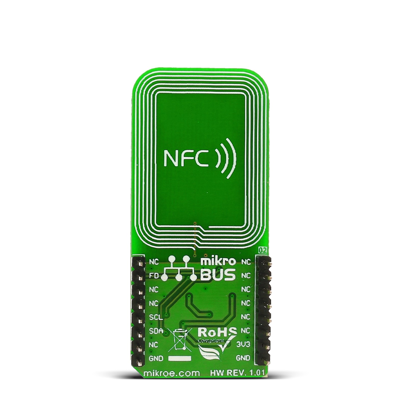
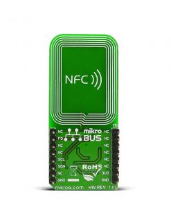
This table shows how the pinout on NFC Tag 2 Click corresponds to the pinout on the mikroBUS™ socket (the latter shown in the two middle columns).
Onboard settings and indicators
Label | Name | Default | Description |
---|---|---|---|
LD1 | PWR | – | Power LED Indicator |
LD2 | PD | – | Field Detection Indicator |
NFC Tag 2 Click electrical specifications
Description | Min | Typ | Max | Unit |
---|---|---|---|---|
Supply Voltage | – | 3.3 | – | V |
External RF Signal Frequency | – | 13.56 | – | MHz |
EEPROM Size | – | 888 | – | bytes |
SRAM Size | – | 64 | – | bytes |