MIC33153 Click
R465.00 ex. VAT
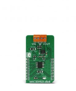
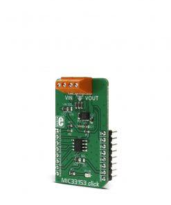
MIC33153 click is a DC-DC adjustable step-down (buck) converter that is designed to deliver a substantial amount of current to very demanding loads, with the voltage output up to 3.5V. The ultra-fast transient response and the ripple free output voltage are some of the main features of this DC-DC step-down converter. The proprietary HyperLight Load™ technology allows very efficient step-down conversion even for very light loads.
This adjustable DC-DC step-down converter click board™ has a very specific field of applications in which it gives the best results. Due to its ripple free voltage output and very high conversion efficiency, it is designed to be used as the power supply for the various portable GPS devices, mobile handsets, portable media and mp3 players, wireless LAN cards and similar applications that demand very clean power supply and high step down DC-DC conversion efficiency factor.
Stock: Lead-time applicable.
| 5+ | R441.75 |
| 10+ | R418.50 |
| 15+ | R395.25 |
| 20+ | R380.37 |
MIC33153 click is a DC-DC adjustable step-down (buck) converter that is designed to deliver a substantial amount of current to very demanding loads, with the voltage output up to 3.5V. The ultra-fast transient response and the ripple free output voltage are some of the main features of this DC-DC step-down converter. The proprietary HyperLight Load™ technology allows very efficient step-down conversion even for very light loads.
This adjustable DC-DC step-down converter click board™ has a very specific field of applications in which it gives the best results. Due to its ripple free voltage output and very high conversion efficiency, it is designed to be used as the power supply for the various portable GPS devices, mobile handsets, portable media and mp3 players, wireless LAN cards and similar applications that demand very clean power supply and high step down DC-DC conversion efficiency factor.
How does it work?
This click uses the MIC33153, a 4MHz DC-DC buck regulator with integrated inductor and Hyperlight Load™ technology, from Microchip. This integrated buck regulator requires a minimal number of external components, including the inductor. This simplifies the design greatly, retaining the advertised electrical characteristics. Also, thermal shutdown and current limit protection features ensure the safe operation, even in case of errors and short circuits.
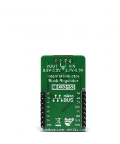
The click operates with the input voltage range from 2.7V up to 5.5V and it is capable to deliver a regulated output ranging from 0.8V to 3.5V, with up to 1.2A. The output voltage is selectable and it is managed by the voltage on the FB pin. This pin is routed to the output of the MCP4921, a 12bit DAC converter from Microchip, with the SPI interface. The voltage on the DAC output affects the FB pin voltage, which in return affects the main output voltage.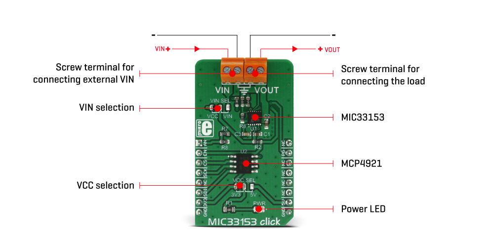
A voltage divider connected between the main output terminal and the GND, allows monitoring the output voltage via the AN pin of the mikroBUS™. This gives an insight of the output voltage condition: if the output voltage deviates from the desired value, the corrected value can be sent to the DAC. MCP4921 DAC converter has its SPI lines routed to the mikroBUS™ so it is enough to just send a new value via the SPI of the click board™ if a correction is needed. Of course, being a buck converter, the click board™ expects higher input voltage than it is set at its output.
The proprietary HyperLight Load™ technology allows to still operate with enough efficiency, when a very light load is connected to the output terminal. Instead of using the continuous PWM signal to operate the DC-DC buck converter, it goes into the discontinuous mode, with the pulse frequency modulation (PFM) signal used for regulating of the output. As the output current rises, the device enters the continuous conducting mode (CCM) with the PWM frequency at 4MHz. The transition is transparent and it happens automatically when the output current rises above a certain level. This level depends on the duty cycle of the internal PWM signal, input and output voltages, PWM frequency and the internal coil inductance, and it is about 200mA for the VIN = 3.6V and VOUT = 1.8V
The EN pin of the MIC33153 is also routed to the mikroBUS™ and it is used to disable the output stage of the DC-DC step down converter. A logic HIGH signal will activate the device, while the logic LOW will put the device in the shutdown mode with very low power consumption. The EN pin is a subject to a soft start circuitry, that reduces the inrush current and prevents the output voltage from overshooting at the start up. The Soft start delay is determined by the capacitor connected to the SS pin and it is fixed to around 300µS for the MIC33153 click. The EN pin is pulled HIGH by the onboard resistor.
The PG pin of the MIC33153 is routed to the INT pin of the mikroBUS™ and it is used to signalize the power good status of the output voltage. It is an open drain output which is pulled low when the output voltage drops under 86%. It reverts to the HIGH logic state, when the output voltage gets to the 92% of its steady state. It can be used to generate the interrupt event on the controller or otherwise signal the output voltage problem. The PG pin is pulled HIGH by the onboard resistor.
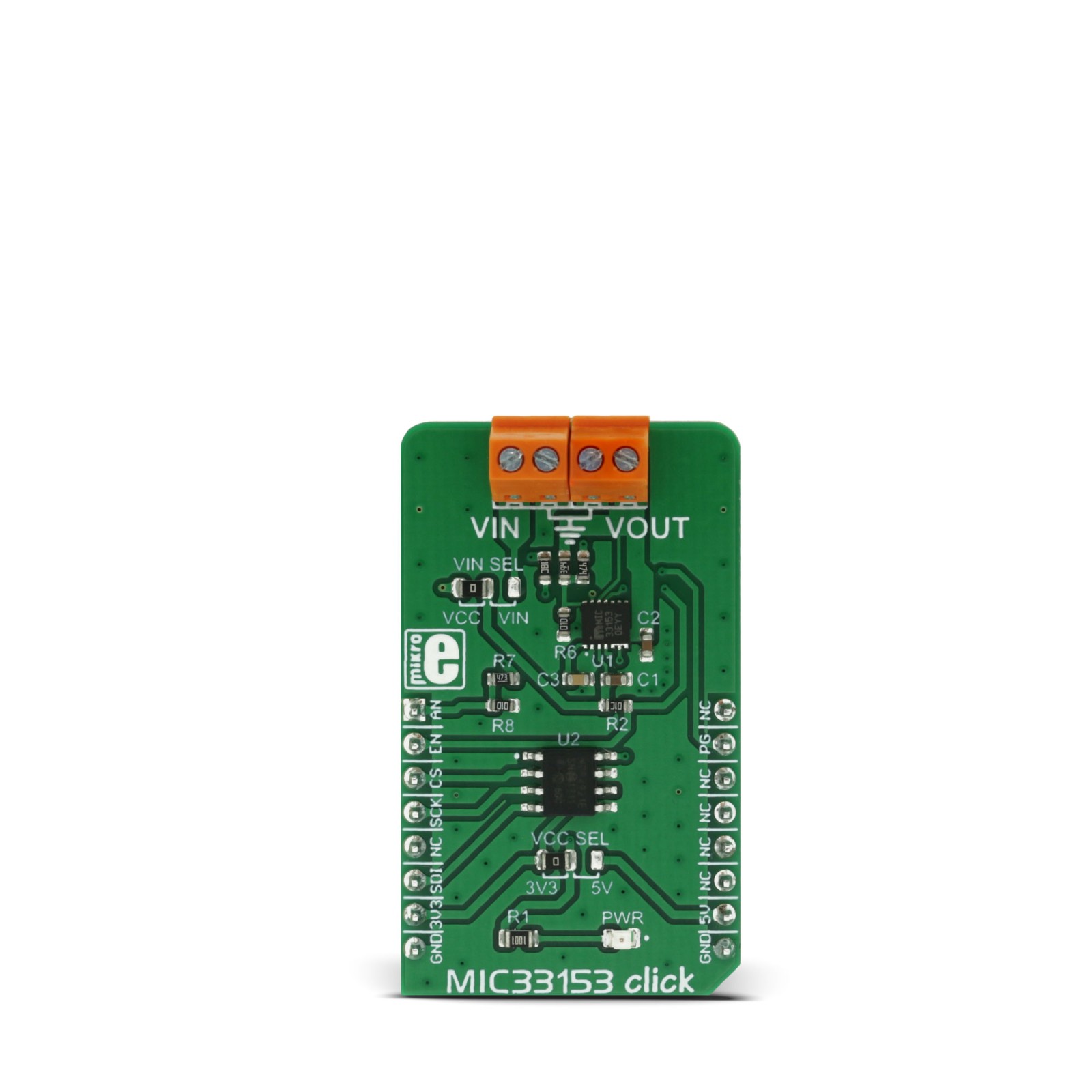
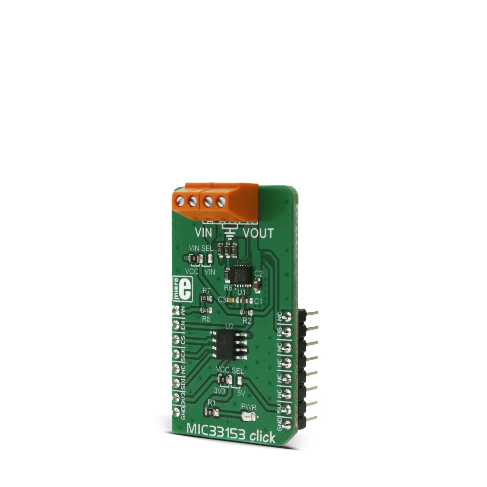
The MIC33153 click has two robust screw terminals for connecting the input and output voltage rails. Instead from the input terminal, the click can use the voltage input from the development system itself if VIN SEL SMD jumper is switched to the VCC position (default jumper position). MIC33153 click can work with both 3.3V and 5V rated MCUs. To select the desired operational voltage, the VCC SEL SMD jumper should be switched to the correct position, indicated by the label – 3.3V or 5V. It should be noted that the selected voltage will be used as the internal voltage supply for the buck converter input, if selected so by the VIN SEL. Also, 3.3V is required regardles of the position of the VCC SEL jumper, since the MCP4921 DAC is powered up from 3.3V rail, directly.
Specifications
Type
Buck
Applications
Power supply for the various portable GPS devices, mobile handsets, portable media and mp3 players, wireless LAN cards and similar applications that demand very clean power supply and high step down DC-DC conversion efficiency factor.
On-board modules
MIC33153 a 4MHz DC-DC buck regulator with integrated inductor and Hyperlight Load™ technology, and MCP4921, a 12bit DAC converter with the SPI interface, both from Microchip.
Key Features
High efficiency and low output voltage ripple throughout the whole load range, soft start feature, thermal shutdown and current limit protection, up to 1.2A of current, HyperLight Load™ technology, adjustable output voltage and power good indication
Interface
Analog,GPIO,SPI
Feature
No ClickID
Compatibility
mikroBUS™
Click board size
M (42.9 x 25.4 mm)
Input Voltage
3.3V or 5V
Pinout diagram
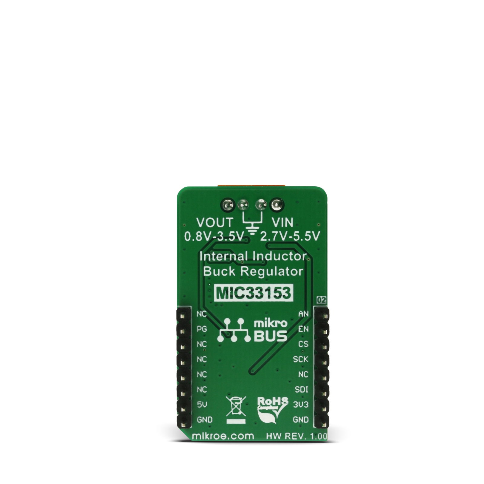
This table shows how the pinout on MIC33153 click corresponds to the pinout on the mikroBUS™ socket (the latter shown in the two middle columns).
MIC33153 click electrical specifications
| Description | Min | Typ | Max | Unit |
|---|---|---|---|---|
| VIN | 2.7 | 5.5 | V | |
| VOUT | 0.8 | 3.5 | V |
Onboard settings and indicators
| Label | Name | Default | Description |
|---|---|---|---|
| LD1 | PWR | – |
Power LED indicator
|
| JP1 | VCC SEL | Left | Power supply voltage selection 3V3/5V, left position 3V3 |
| JP2 | VIN SEL | Left | Power supply for the buck converter selection VCC/VIN, left position VCC |
| TB1 | VIN | – | Screw terminal for connecting external VIN |
| TB2 | VOUT | – | Screw terminal for connecting the load |
Software support
We provide a library for MIC15333 click on our LibStock page, as well as a demo application (example), developed using MikroElektronika compilers and mikroSDK. The provided click library is mikroSDK standard compliant. The demo application can run on all the main MikroElektronika development boards.
Library Description
Initializes and defines SPI driver, defines driver’s function that writes a 12-bit value in DAC, and that causes the output voltage to be set at the determined value. This function checks PG (INT) pin state that shows the result of comparing the output voltage with its steady-state voltage. It also enables or disables the output voltage. Check the documentation for more details.
Key functions
void mic33153_writeDAC(const uint16_t valueDAC)– Function writes 12-bit value to DAC
void mic33153_enableOut(uint8_t state)– Function enables or disables output voltage
uint8_t mic33153_checkPowerGood(void)– Function checks state of PG (INT) pin
Examples Description
The demo application is composed of three sections:
- System Initialization – Initializes peripherals and pins.
- Application Initialization – Initializes click driver.
- Application Task – Activates the output voltage of the device, writes DAC value which sets output voltage to 2V, and checks PG (Power Good) pin which compares the output voltage with its steady state voltage. MIC33153 click is tested on load with a current output value of 20mA.
void applicationTask()
{
    uint8_t powerGood;

    mic33153_enableOut(_MIC33153_OUT_ENABLE);

    mic33153_writeDAC(_MIC33153_VOLTAGE_2000MV);

    powerGood = mic33153_checkPowerGood();

    if(powerGood && i)
    {
        mikrobus_logWrite("Output voltage is above 92% of its steady state voltage.", _LOG_LINE);
        i = 0;
    }else if((powerGood == 0) && (i == 0))
    {
        mikrobus_logWrite("Output voltage is below 86% of its steady state voltage.", _LOG_LINE);
        i = 1;
    }

    Delay_ms(2000);
}
The full application code, and ready to use projects can be found on our LibStock page.
Additional notes and information
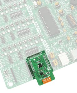
Depending on the development board you are using, you may need USB UART click, USB UART 2 click or RS232 click to connect to your PC, for development systems with no UART to USB interface available on the board. The terminal available in all MikroElektronika compilers, or any other terminal application of your choice, can be used to read the message.
mikroSDK
This click board is supported with mikroSDK - MikroElektronika Software Development Kit. To ensure proper operation of mikroSDK compliant click board demo applications, mikroSDK should be downloaded from the LibStock and installed for the compiler you are using.
For more information about mikroSDK, visit the official page.
Resources
Downloads
| Weight | 18 g |
|---|---|
| Brand | MikroElektronika |

