How does it work?
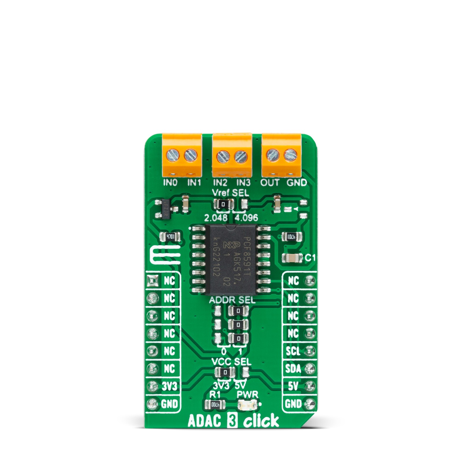
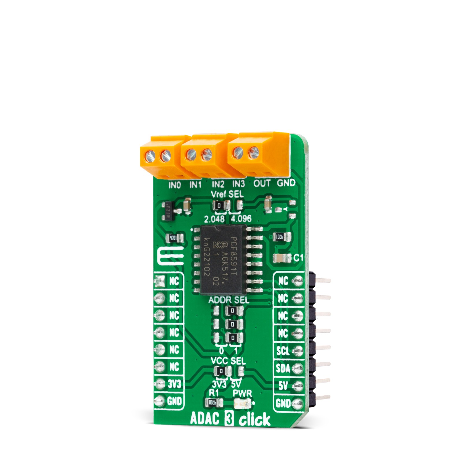
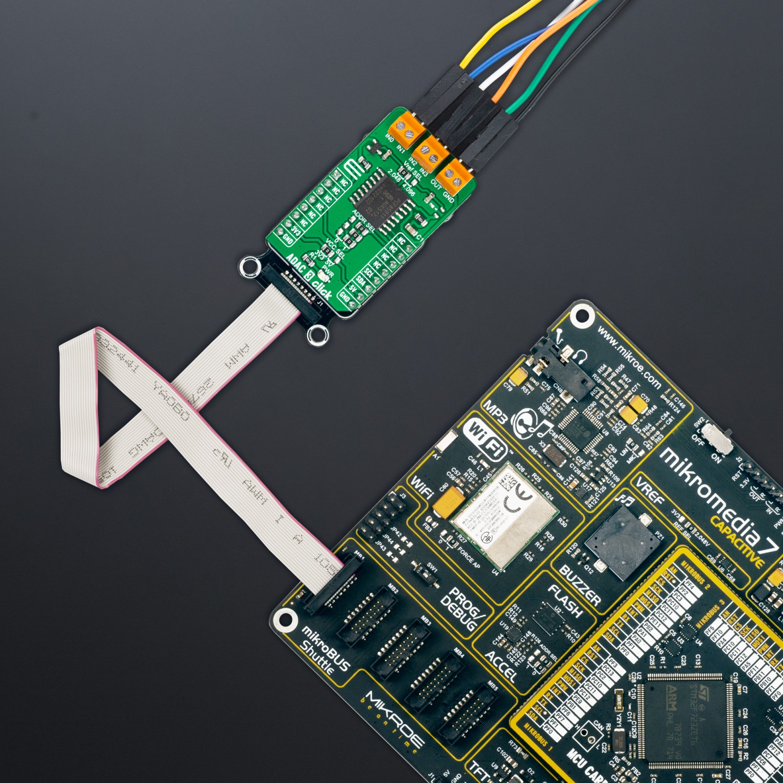
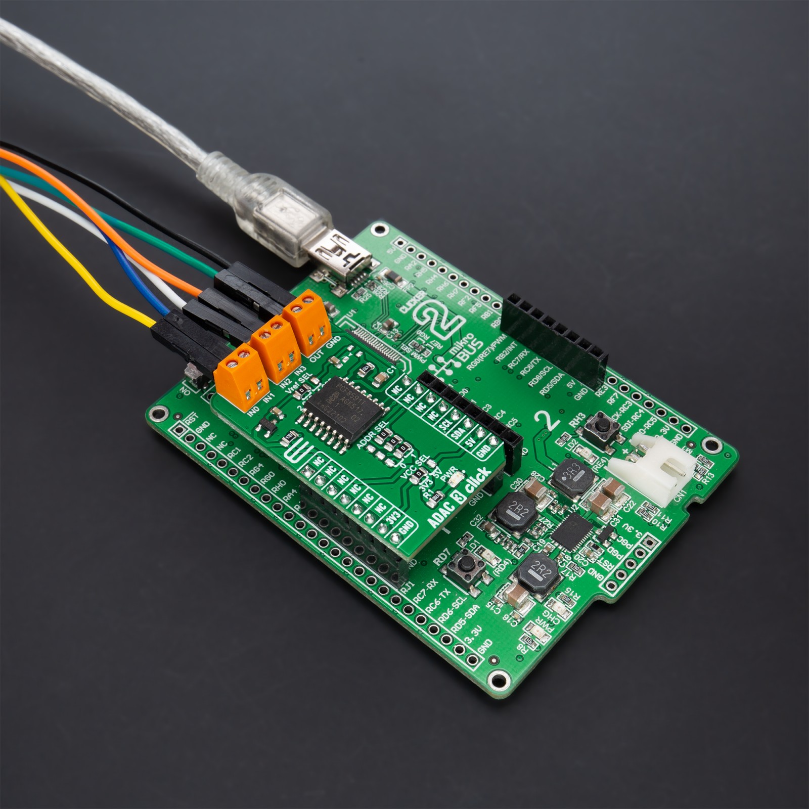
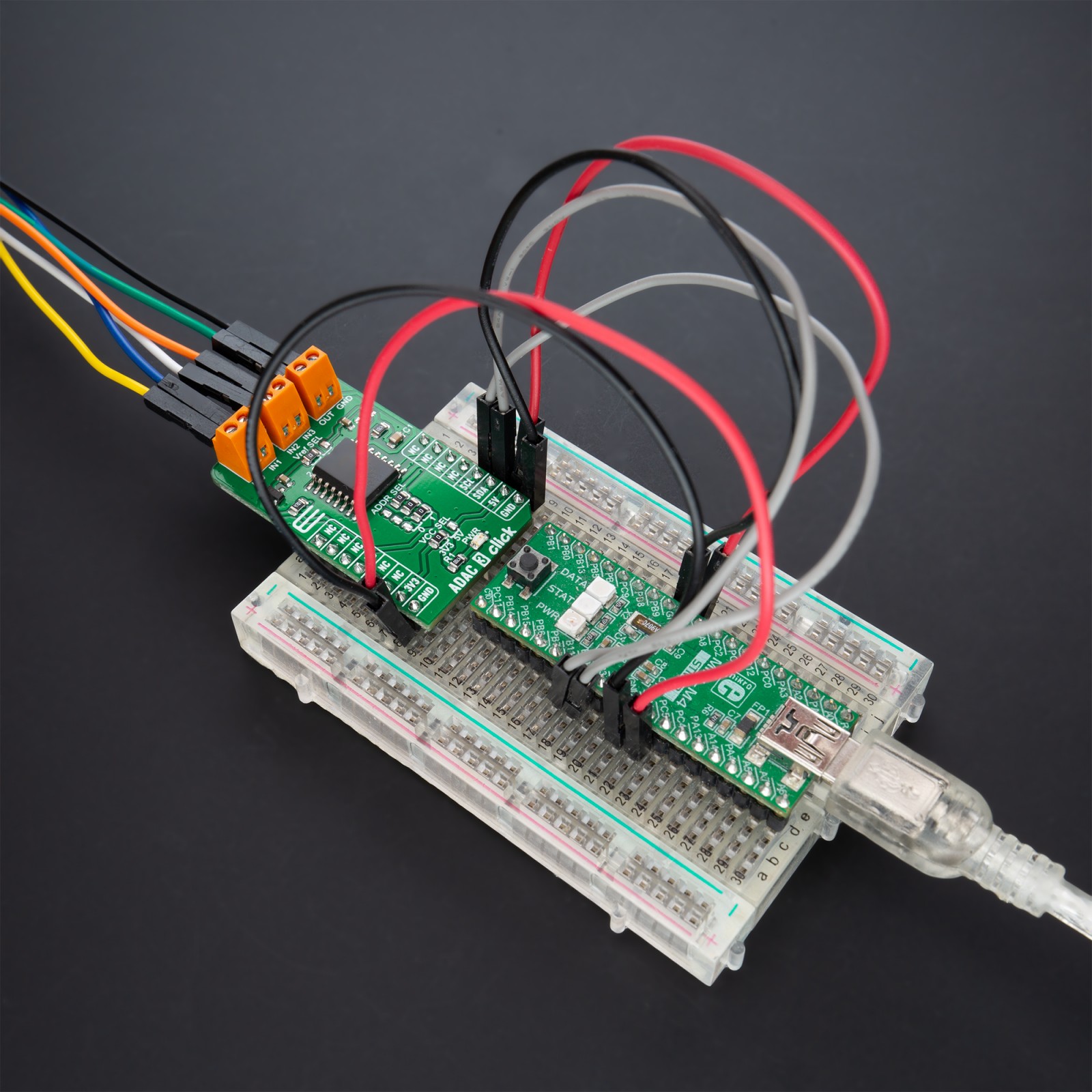
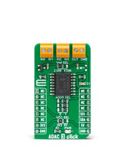
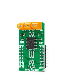
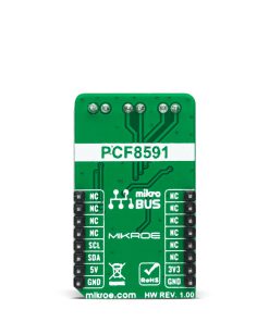
ADAC 3 Click as its foundation uses the PCF8591, a low-power CMOS data acquisition device from NXP Semiconductors. The PCF8591 comes with four analog inputs configurable as single-ended or differential inputs used to measure voltages, alongside one analog output representing an 8-bit digital-to-analog converter. In addition to measuring voltage, the user can create them as desired and even use DAC and ADC together to generate an input to a circuit and measure the results with the ADC, making it suitable for various control, monitoring, or measurement applications. By its internal structure, the PCF8591 also consists of an analog input multiplexing circuit, an on-chip track and hold function, alongside a serial interface block.
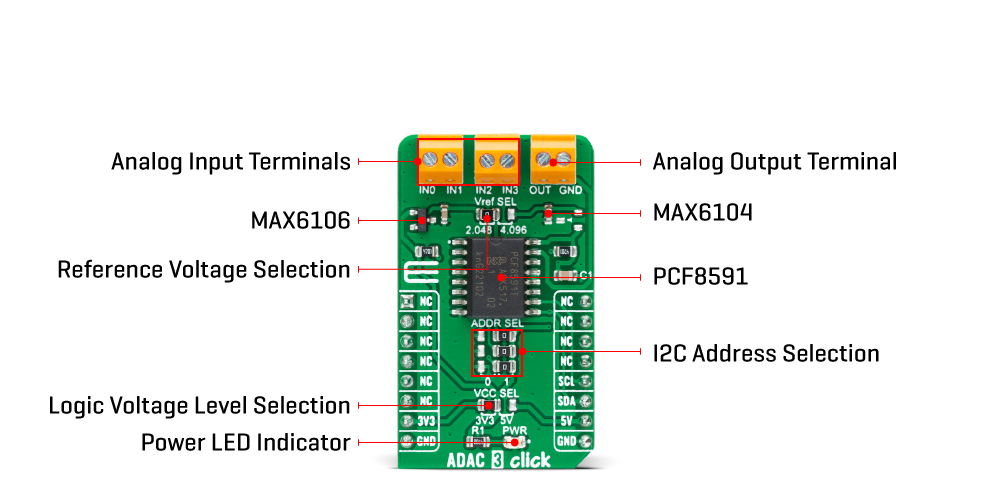
This Click board™ communicates with MCU using the standard I2C 2-Wire interface with a maximum clock frequency of 100kHz. The PCF8591 has a 7-bit slave address with the first four MSBs fixed to 1001. The address pins A0, A1, and A2, are programmed by the user and determine the value of the last three LSBs of the slave address, which can be selected by positioning onboard SMD jumpers labeled as ADDR SEL to an appropriate position marked as 0 or 1.
Besides, the user can choose the PCF8591 reference voltage value by positioning the SMD jumper labeled VREF SEL to a proper position, choosing between 2,048 and 4,096V provided by MAX6104 and MAX6106.
This Click board™ can operate with both 3.3V and 5V logic voltage levels selected via the VCC SEL jumper. This way, it is allowed for both 3.3V and 5V capable MCUs to use the communication lines properly. However, the Click board™ comes equipped with a library containing easy-to-use functions and an example code that can be used, as a reference, for further development.
Specifications
Type
ADC-DAC
Applications
Can be used for various control, monitoring, or measurement applications
On-board modules
PCF8591 – low-power CMOS data acquisition device from NXP Semiconductors
Key Features
Low power consumption, combo solution with four analog inputs and one analog output, 8-bit successive approximation A/D conversion, I2C serial interface, analog inputs configurable as single ended or differential inputs, on-chip track and hold circuit, and more
Interface
I2C
Feature
No ClickID
Compatibility
mikroBUS™
Click board size
M (42.9 x 25.4 mm)
Input Voltage
3.3V or 5V
Pinout diagram
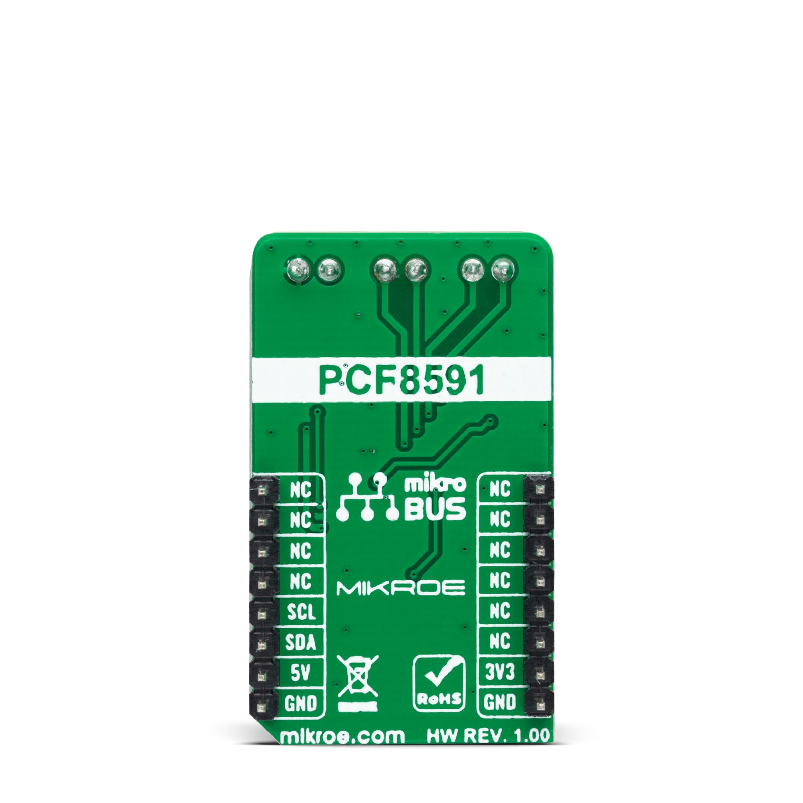
This table shows how the pinout on ADAC 3 Click corresponds to the pinout on the mikroBUS™ socket (the latter shown in the two middle columns).
Onboard settings and indicators
Label | Name | Default | Description |
---|---|---|---|
LD1 | PWR | – | Power LED Indicator |
JP1 | VCC SEL | Left | Logic Level Voltage Selection 3V3/5V: Left position 3V3, Right position 5V |
JP2-JP4 | ADDR SEL | Right | I2C Address Selection 0/1: Left position 0, Right position 1 |
JP5 | VREF SEL | Left | Reference Voltage Selection 2.048/4.096: Left position 2.048, Right position 4.096 |
ADAC 3 Click electrical specifications
Description | Min | Typ | Max | Unit |
---|---|---|---|---|
Supply Voltage | 3.3 | – | 5 | V |
Analog Input Voltage | 0 | – | 5 | V |
Analog Output Voltage | 0 | – | 5 | V |
Resolution | – | 8 | – | bit |
Operating Temperature Range | -40 | +25 | +85 | °C |
Software Support
We provide a library for the ADAC 3 Click as well as a demo application (example), developed using MikroElektronika compilers. The demo can run on all the main MikroElektronika development boards.
Package can be downloaded/installed directly from NECTO Studio Package Manager(recommended way), downloaded from our LibStock™ or found on Mikroe github account.
Library Description
This library contains API for ADAC 3 Click driver.
Key functions
-
adac3_write_control
This function writes a control byte by using I2C serial interface. -
adac3_write_dac
This function writes a DAC byte by using I2C serial interface. -
adac3_read_adc
This function reads the AD conversion byte by using I2C serial interface.
Example Description
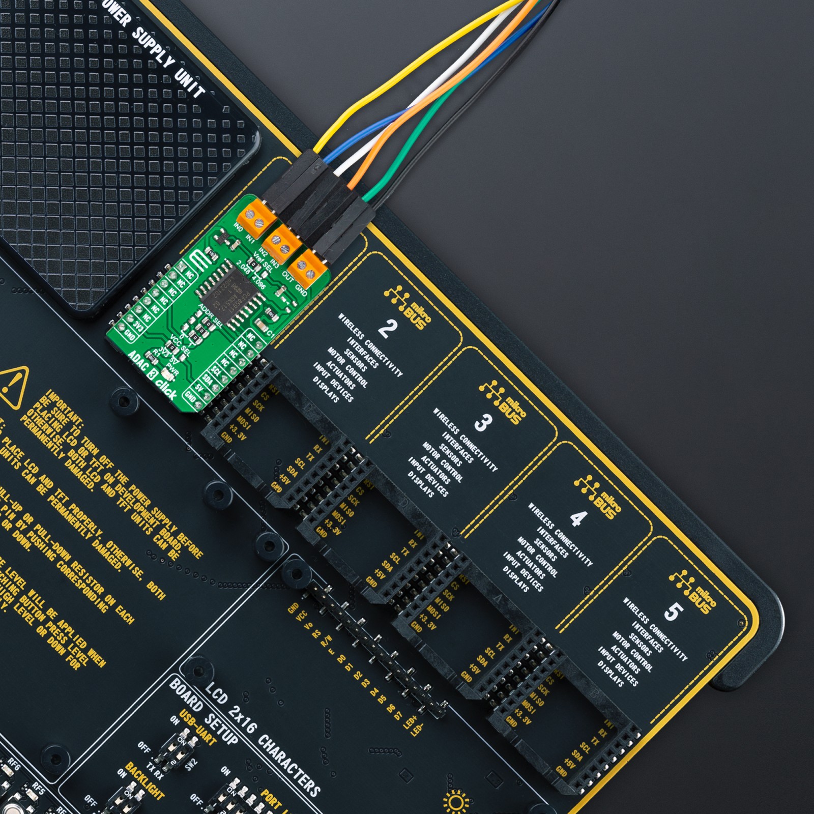
This example demonstrates the use of ADAC 3 click board by setting the DAC output and reading the ADC results from 2 single-ended channels (AIN0, AIN1) and from a differential channel (AIN2+, AIN3-).
void application_task ( void )
{
static uint8_t dac = 0;
uint8_t ain0, ain1, ain2_ain3_diff;
if ( ADAC3_OK == adac3_write_dac ( &adac3, dac ) )
{
log_printf ( &logger, " DAC : %u mVrn",
( uint16_t ) ( ( ADAC3_VREF_2048mV / ADAC3_RESOLUTION ) * dac++ ) );
}
if ( ADAC3_OK == adac3_read_adc ( &adac3, &ain0 ) )
{
log_printf ( &logger, " AIN0+: %u mVrn",
( uint16_t ) ( ( ADAC3_VREF_2048mV / ADAC3_RESOLUTION ) * ain0 ) );
}
if ( ADAC3_OK == adac3_read_adc ( &adac3, &ain1 ) )
{
log_printf ( &logger, " AIN1+: %u mVrn",
( uint16_t ) ( ( ADAC3_VREF_2048mV / ADAC3_RESOLUTION ) * ain1 ) );
}
if ( ADAC3_OK == adac3_read_adc ( &adac3, &ain2_ain3_diff ) )
{
log_printf ( &logger, " AIN2+ - AIN3-: %d mVrnn",
( int16_t ) ( ( ADAC3_VREF_2048mV / ADAC3_RESOLUTION ) * ( int8_t ) ain2_ain3_diff ) );
}
Delay_ms ( 100 );
}
The full application code, and ready to use projects can be installed directly from NECTO Studio Package Manager(recommended way), downloaded from our LibStock™ or found on Mikroe github account.
Other Mikroe Libraries used in the example:
- MikroSDK.Board
- MikroSDK.Log
- Click.ADAC3
Additional notes and informations
Depending on the development board you are using, you may need USB UART click, USB UART 2 Click or RS232 Click to connect to your PC, for development systems with no UART to USB interface available on the board. UART terminal is available in all MikroElektronika compilers.
mikroSDK
This Click board™ is supported with mikroSDK – MikroElektronika Software Development Kit. To ensure proper operation of mikroSDK compliant Click board™ demo applications, mikroSDK should be downloaded from the LibStock and installed for the compiler you are using.
For more information about mikroSDK, visit the official page.